This is an introduction to the ADDAC203 REV.02 CV Mapping by ADDAC System, available at Takazudo Modular.
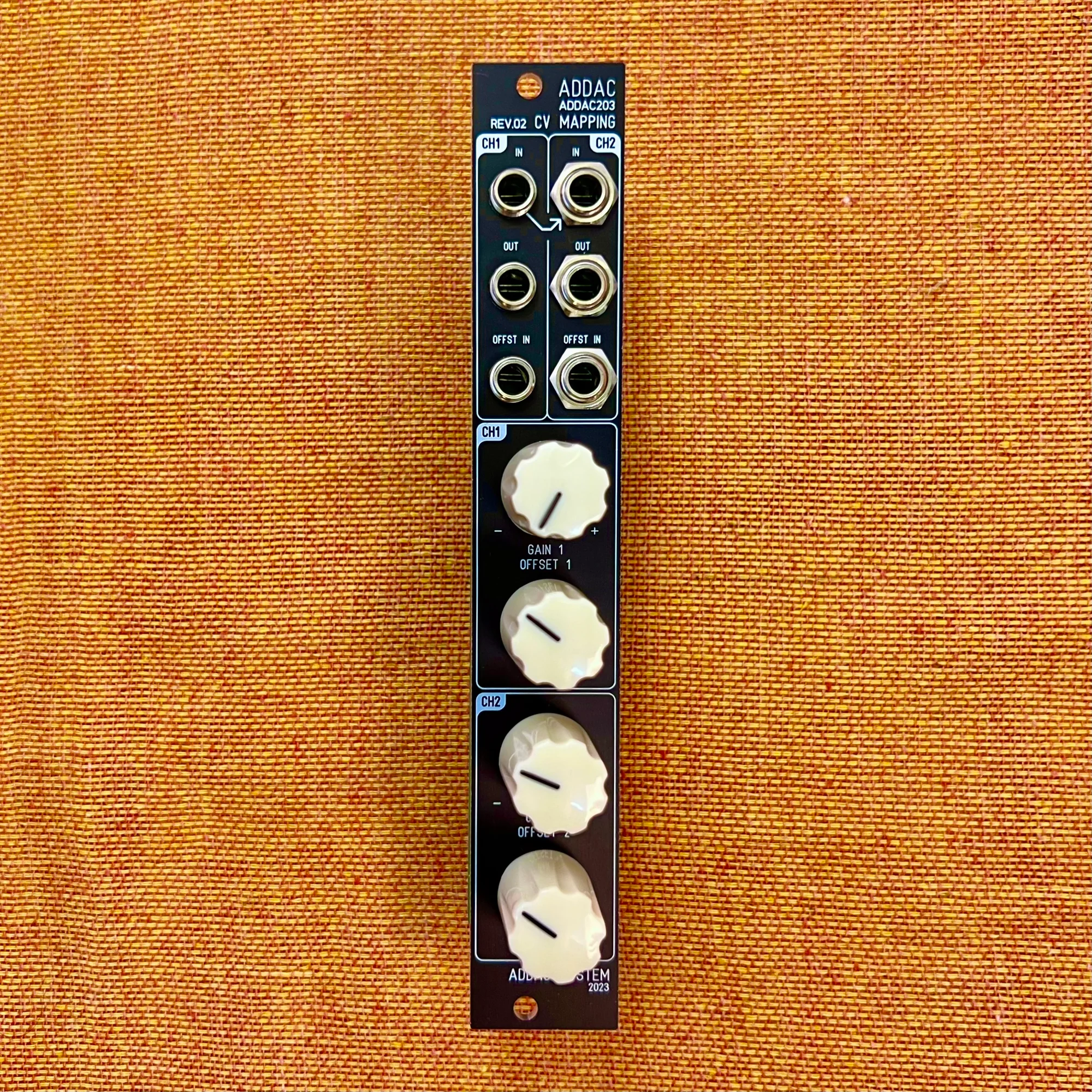
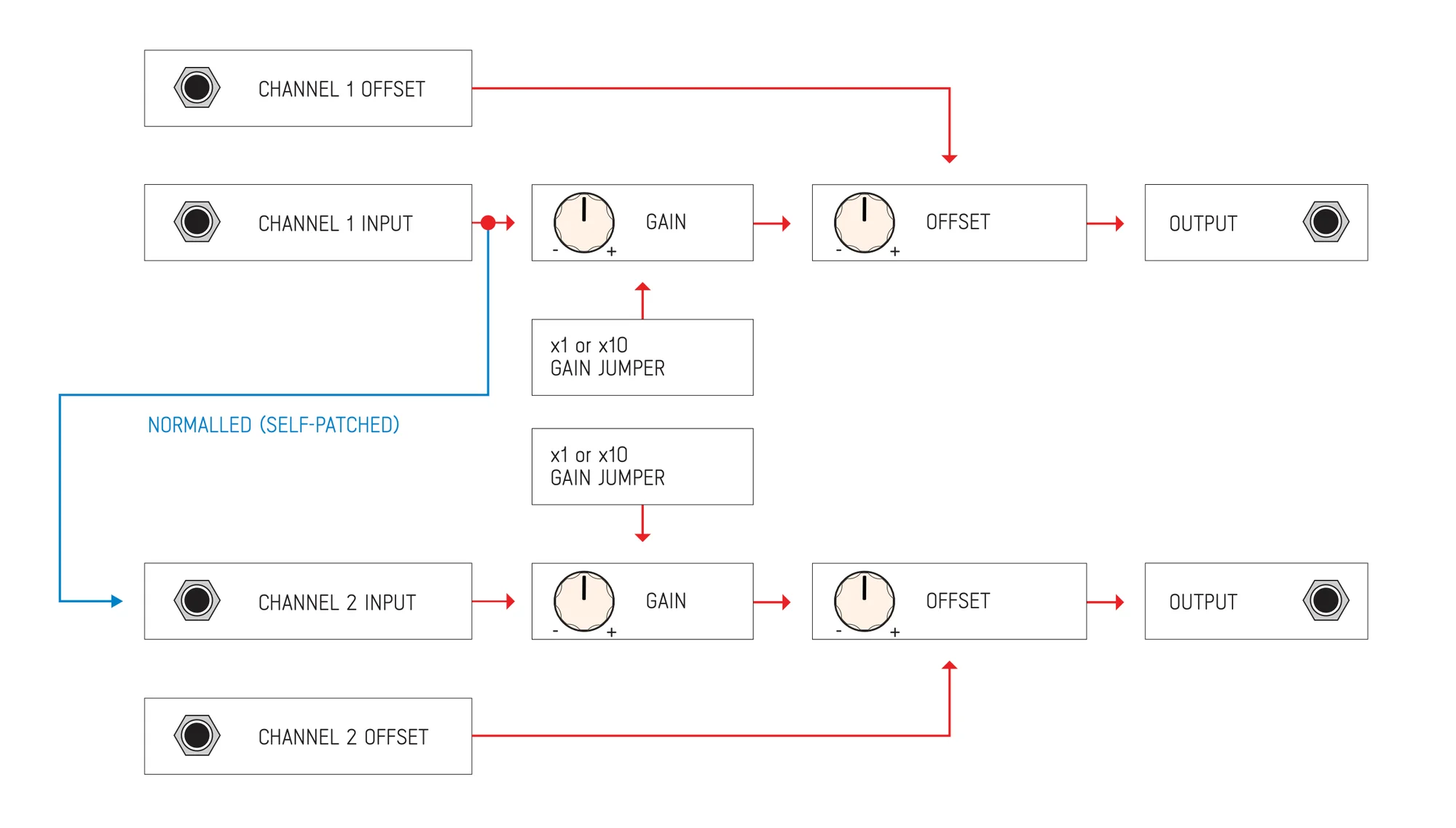
The ADDAC203 REV.02 CV Mapping is a dual-channel CV adjustment module. In addition to attenuating/inverting input CV, it can also offset. It further features a CV input jack for offset and the ability to change the attenuator’s maximum amplification to 10x gain.
This product is available as an assembled unit built by ADDAC System, as well as a DIY kit.
Available for purchase below.
- Product Photos: Assembled
- Product Photos: DIY Kit
- Features of the ADDAC203 REV.02 CV Mapping
- CV Change Examples Before and After Processing
- Use Cases for the ADDAC203 REV.02 CV Mapping
- Technical Specifications
- Included Accessories
- Manual
- DIY Guide
Product Photos: Assembled

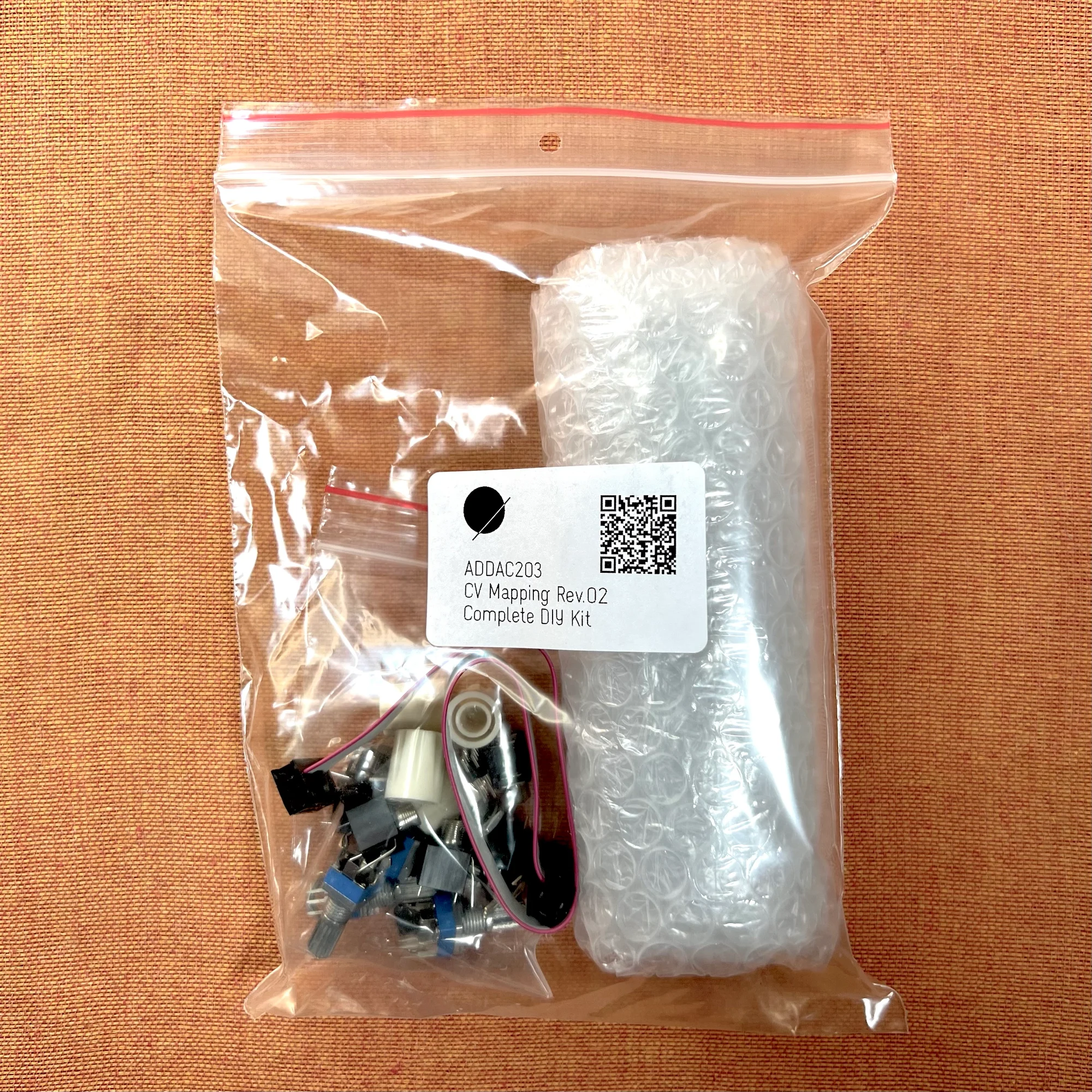
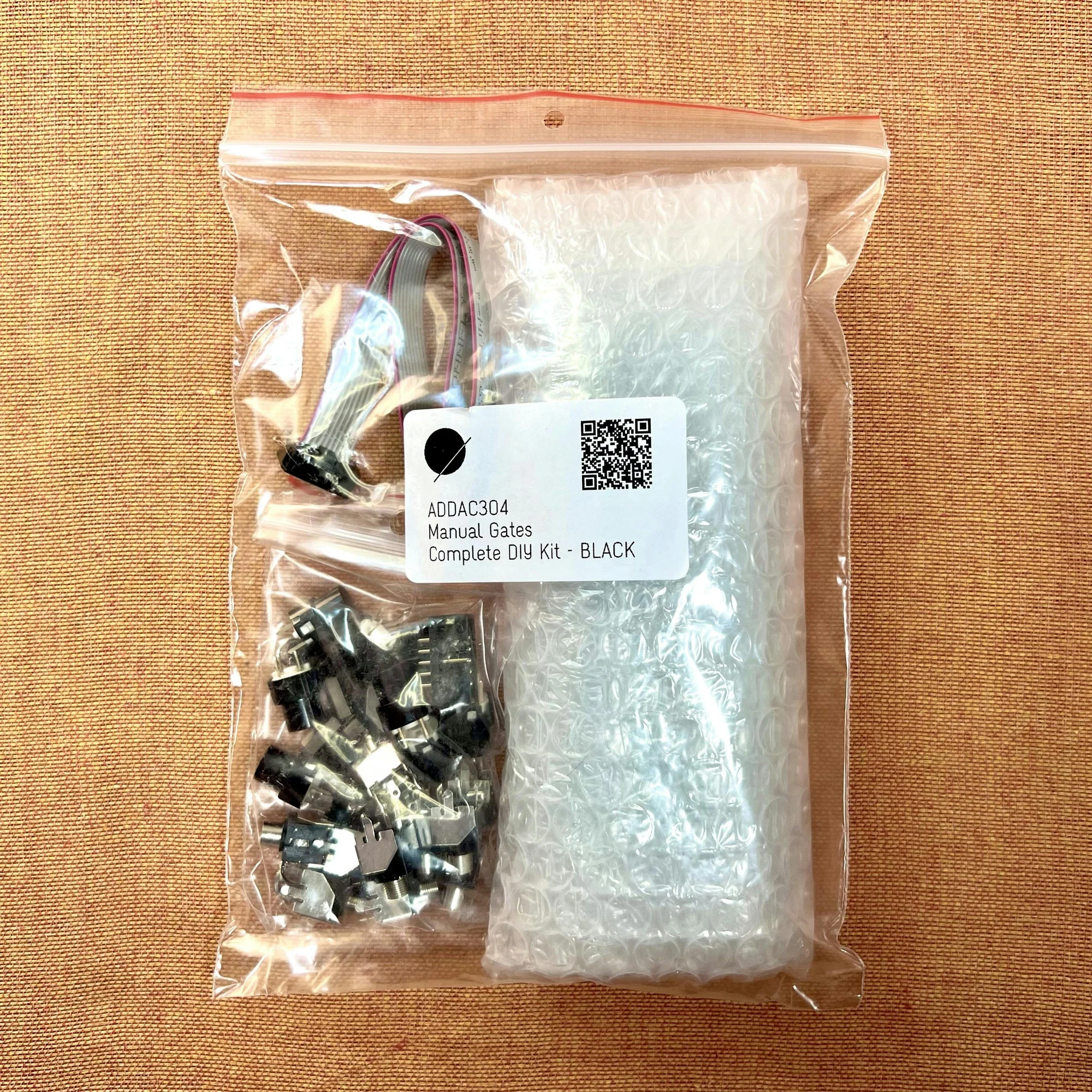
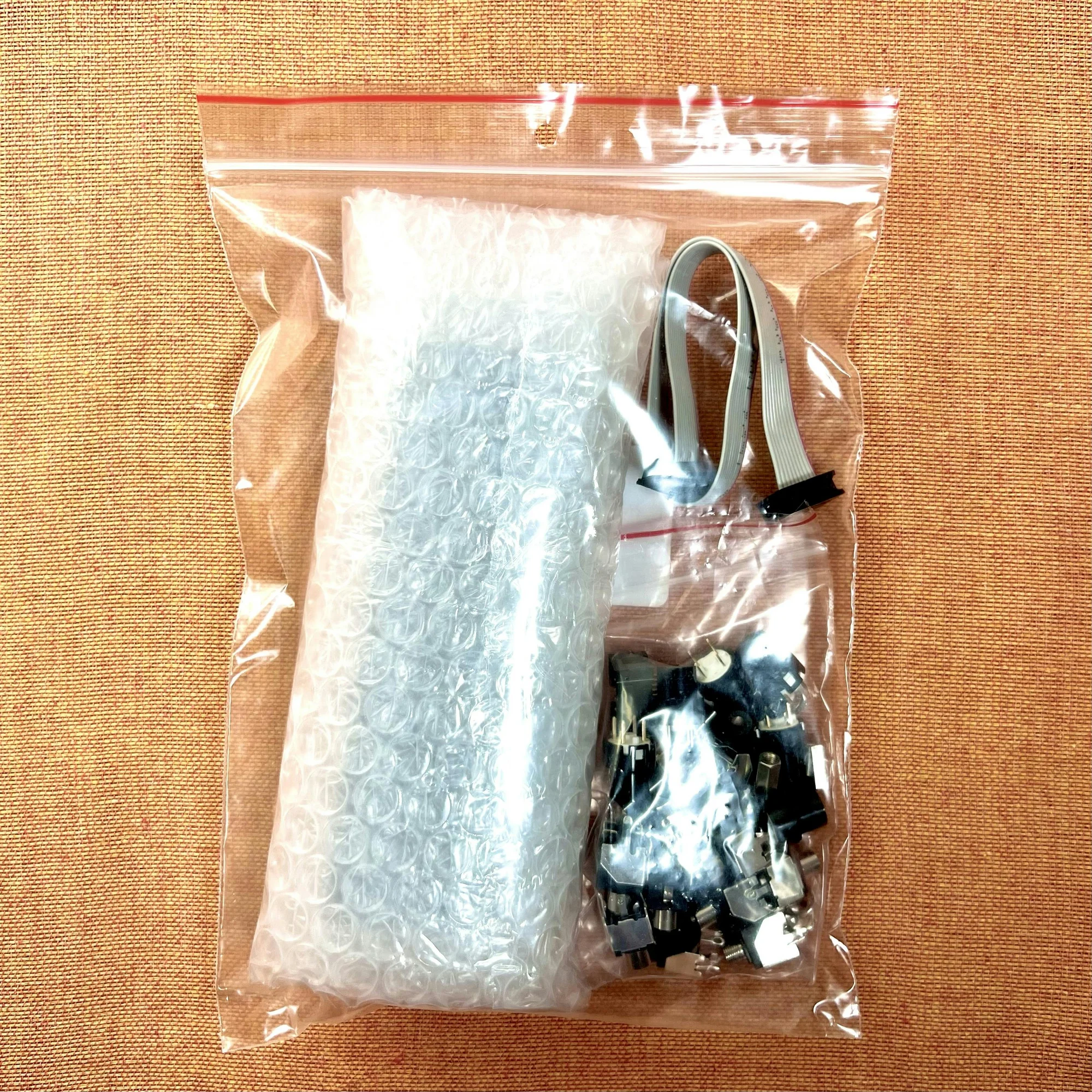
Product Photos: DIY Kit
Features of the ADDAC203 REV.02 CV Mapping
The ADDAC203 REV.02 CV Mapping is a module for CV attenuverting/inverting and offsetting. For example, if CV output from a sequencer or LFO has too wide a swing, you can attenuate/invert it to adjust, or offset it to shift the voltage to your desired range.
When there’s no input, the OFFSET knob position allows it to output a fixed voltage of 0V to 5V. Additionally, separate from the CV input jack, it has a CV input jack for offset, enabling simple CV mixing with this module alone.
The left channel’s CV Input is normalled to the right channel’s CV Input, so when no input is connected to the right channel, the left channel’s CV is also fed to the right channel.
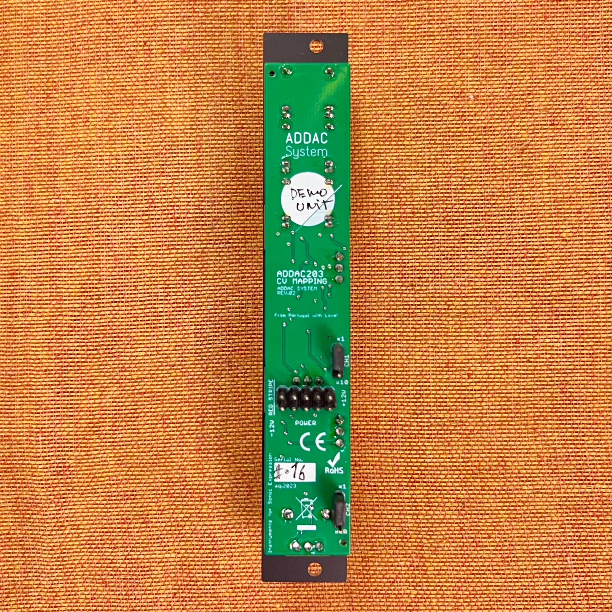
In its default state, the GAIN knob operates as an attenuverter and does not amplify the input signal. However, by switching a jumper on the back, you can change it to amplify the input signal up to 10x.
Compact at 4HP, yet featuring comfortably sized knobs that are easy to operate. Combining the attenuverter and offset you’d want when you need to control CV, plus additional thoughtful features packed in — this is a module we’d highly recommend for anyone looking to experiment with CV control in their modular system.
CV Change Examples Before and After Processing
The official manual contains diagrams showing how CV is processed, which are quite easy to understand. Here they are with brief explanations.
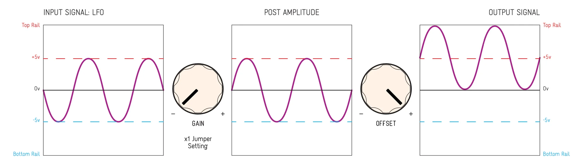
Example 1: GAIN 100%, OFFSET +5V
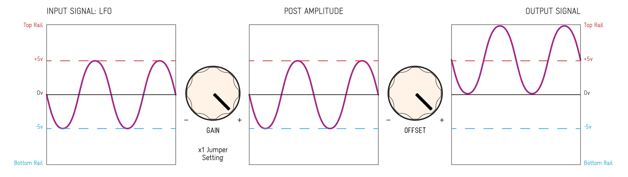
This example shows a sine wave LFO fed into the Input with the GAIN knob turned fully clockwise and the OFFSET knob also turned fully clockwise.
With GAIN turned fully clockwise, the attenuverter does not modify the signal — it maintains 100% of the voltage swing. With the OFFSET knob also turned fully clockwise, the voltage is raised by 5V.
As a result, a sine wave oscillating between -5V and +5V maintains the same swing width but now oscillates between 0V and +10V.
Example 2: GAIN -100%, OFFSET +5V
This example shows a sine wave LFO fed into the Input with the GAIN knob turned fully counter-clockwise and the OFFSET knob turned fully clockwise.
The difference from Example 1 is the GAIN knob position. Here, the attenuverter inverts the signal by 100%, so positive voltage portions of the input sine wave become negative (maintaining the same absolute value), and vice versa. Then with the OFFSET knob fully clockwise, the voltage is raised by 5V.
As a result, the sine wave that was oscillating between -5V and +5V now oscillates between 0V and +10V with an inverted phase.
Example 3: GAIN +100%, OFFSET +5V (Jumper set to 10x)
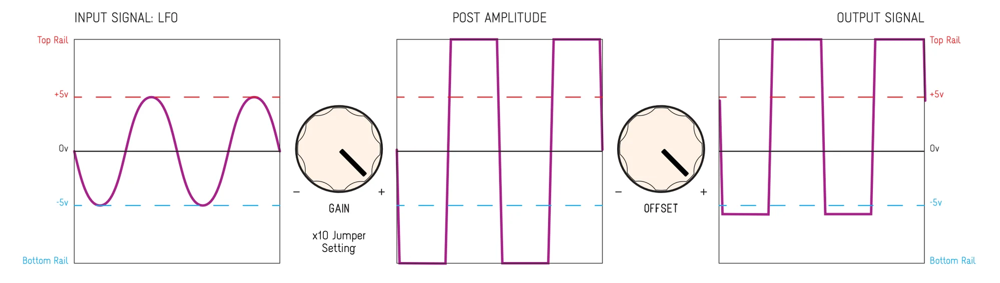
This example shows the jumper on the back of the module switched to 10x, with both knobs positioned the same as Example 1 — GAIN knob fully clockwise and OFFSET knob fully clockwise — and a sine wave LFO fed into the Input.
In Example 1, turning the GAIN knob fully clockwise meant 100% of the input signal passed through unchanged. In Example 3, the jumper setting causes the signal to be amplified 10x. However, this doesn’t suddenly produce 50V — the signal clips at the maximum/minimum voltage the components can handle*.
With the OFFSET knob raising the voltage by 5V based on its position, and the voltage maintaining its clipped state, the positive direction clips near the maximum voltage while the negative direction doesn’t drop below around -5V.
The result is an irregularly shaped waveform close to a square wave.
*While not explicitly stated, it can be assumed to be approximately +/-12V.
Example 4: GAIN Zero, OFFSET +5V
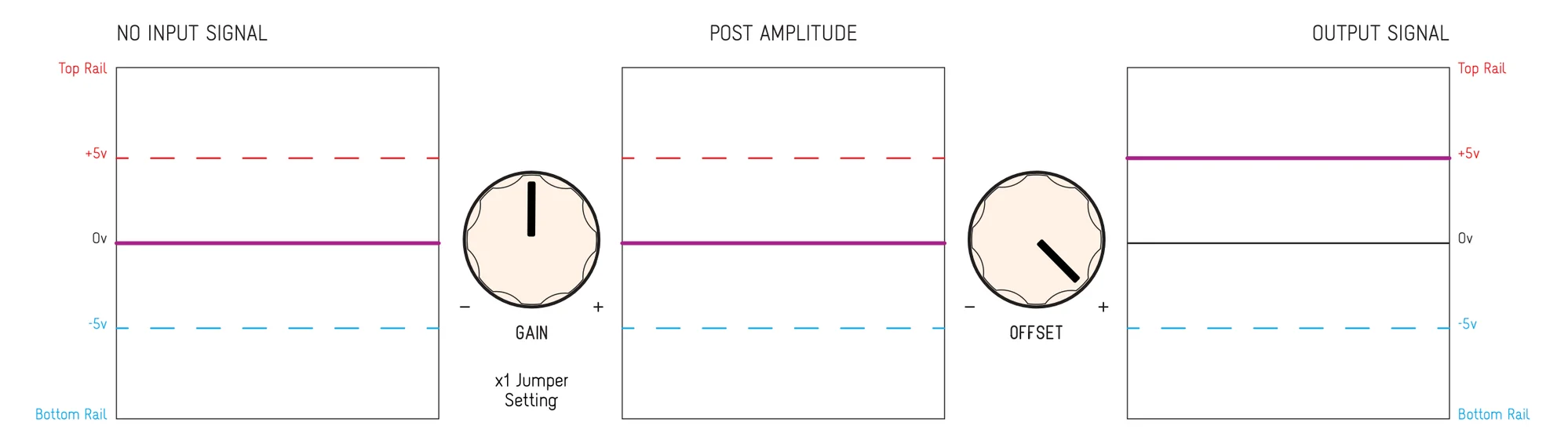
This example shows no input signal, with the GAIN knob at center and the OFFSET knob turned fully clockwise.
In this example, since there’s no input signal, the GAIN knob position is irrelevant. However, with the OFFSET knob fully clockwise, the voltage is raised by +5V.
The result is a fixed voltage output of 5V (0V + 5V).
Example 5: GAIN Zero, OFFSET -5V
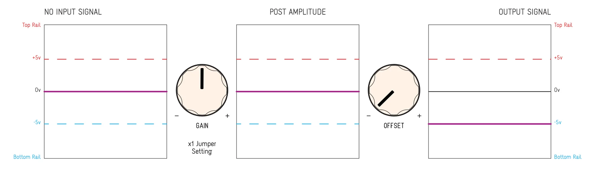
This example is the reverse of Example 4 — the OFFSET knob is turned fully counter-clockwise, outputting a fixed voltage of -5V.
These are the examples of CV before and after processing.
Use Cases for the ADDAC203 REV.02 CV Mapping
For those who regularly process CV to create various sounds, I believe you’ll appreciate the compact, just-right feel of this module. For those less familiar with such concepts, the explanation above might seem complicated.
However, one of the joys of modular synthesis that I personally appreciate is exactly this kind of seemingly subtle CV control to shape the sounds you want. Combined with a quantizer and sequencer, figuring out how to patch things to achieve the desired result — this kind of trial and error is where utility modules like this really shine.
While introducing this module alone can’t fully convey the message that modular synthesis is fun, I hope you’ll get to experience the joy of modular synthesis that emerges when combining it with a sequencer and other modules.
I plan to create videos and explanations that convey this kind of nuance, so please continue to check in with Takazudo Modular.
Technical Specifications
- Width: 4HP
- Depth: 25mm
- Power consumption: 40mA +12V / 40mA -12V
Included Accessories
- Power ribbon cable
- Screws
Manual
The manual is available on the official website below.
DIY Guide
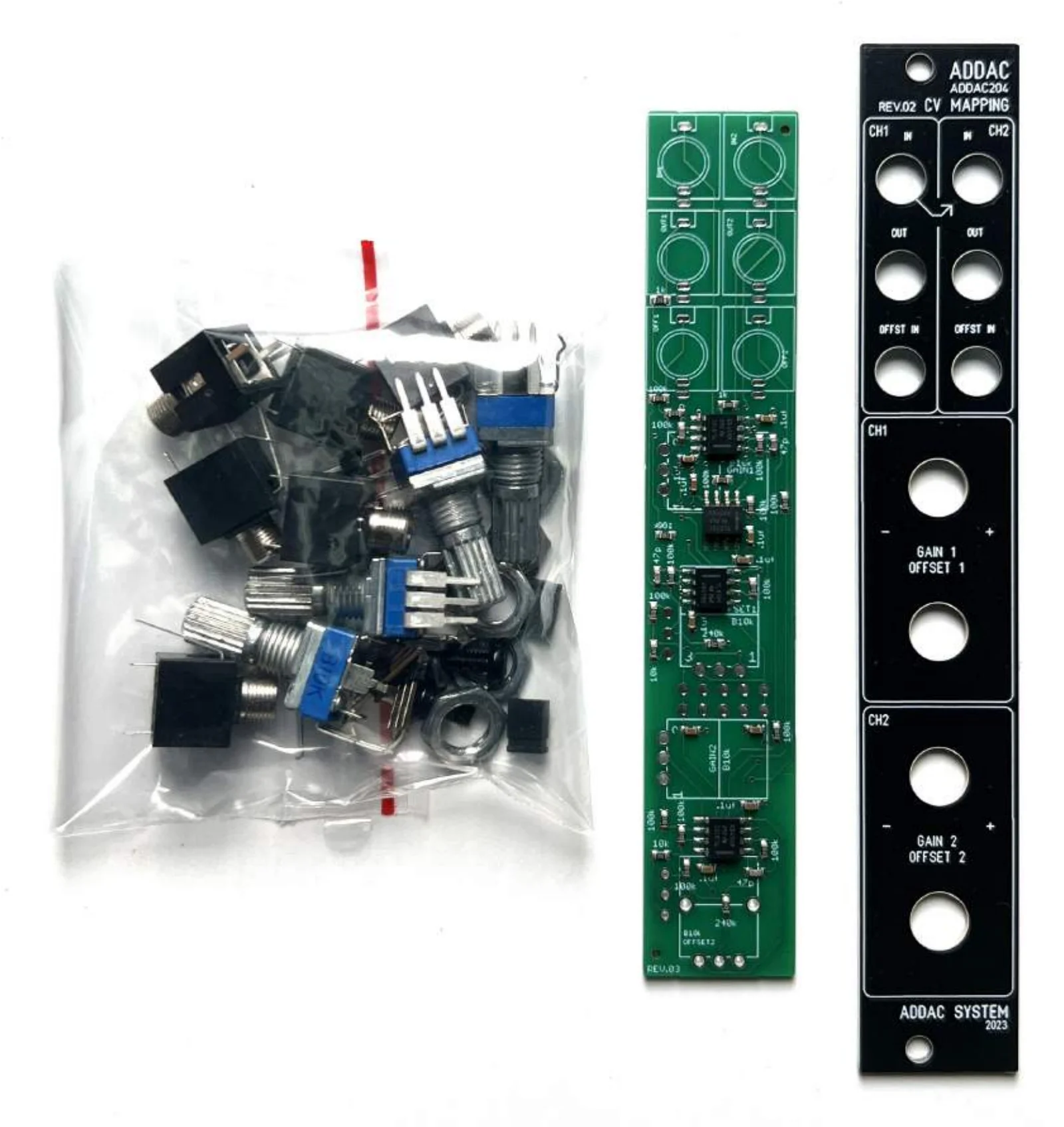
The DIY kit includes the panel, PCB, all components, power ribbon cable, and mounting screws.
ADDAC System provides detailed DIY guides on their website. Please refer to the guide below when assembling your kit.
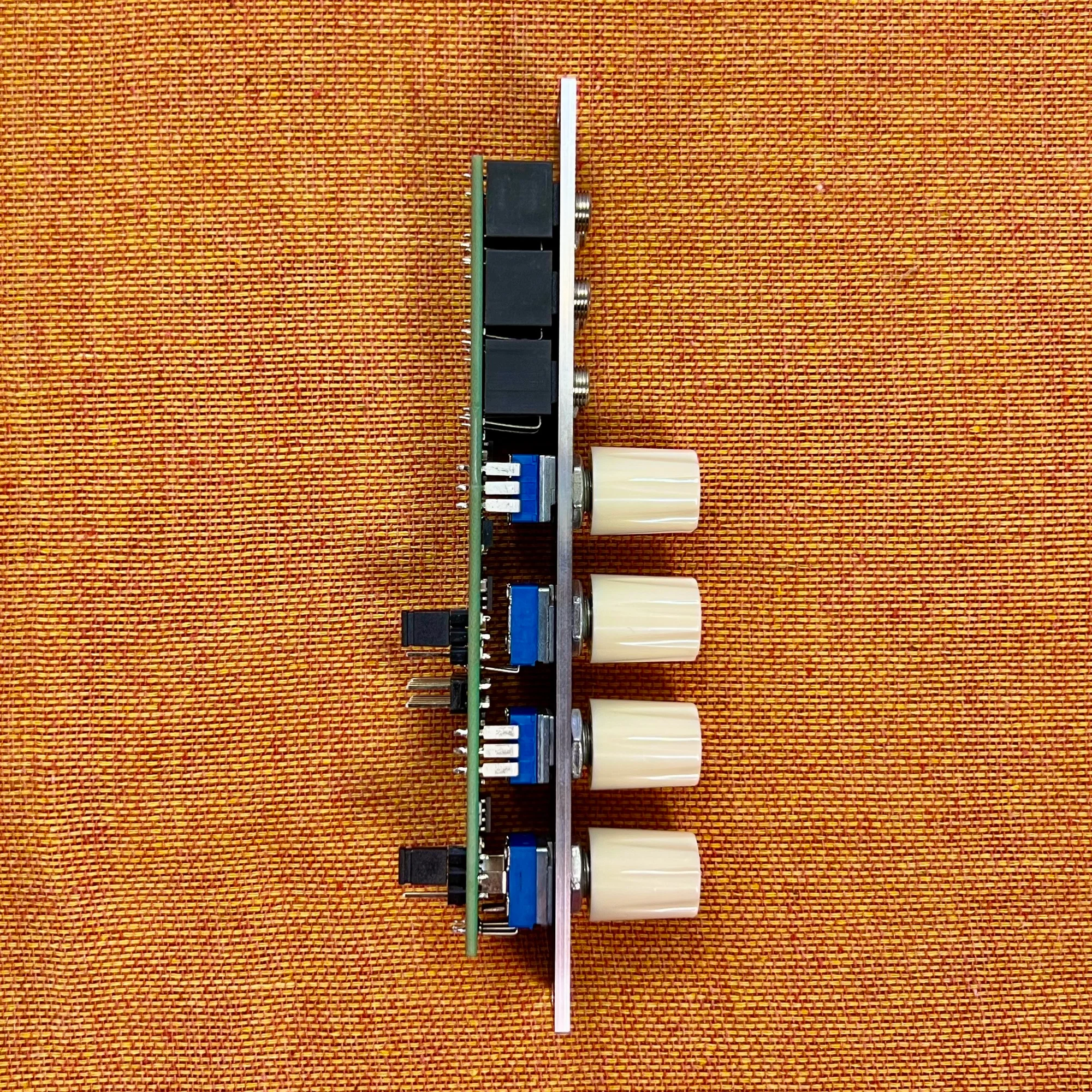
This module uses many very small parts (SMD parts), but these come pre-soldered to the PCB. The kit is designed so that you only need to solder the relatively larger, easier-to-handle through-hole parts to complete the assembly.
Assembly Impressions
I (Takazudo) assembled this kit myself. One point to note is that while this kit only requires you to attach through-hole components as described above, the component density on the board is quite high.
This module fits within 4HP width and 25mm depth, so the spacing between components is quite tight and the solder pads are quite small. You need to be careful not to accidentally touch the fine pre-soldered components with your iron. If you have a fine-tipped soldering iron meant for SMD work, it might be safer to use that. A magnifying glass would also be helpful given how tiny things are.
モジュラーシンセのDIYとは?
モジュラーシンセサイザーのDIYについて詳しくご存じない方向けに、以下にDIYの導入的なコラムを用意しました。DIYについてご興味のある方、始めてみようと思う方は、是非ご参照いただければと。
また、組み立てに際して不明点や不安な点がございましたら、以下Takazudo Modularのdiscordチャンネルにてお気軽にご質問等、頂ければと思います。
ADDAC Systemについて
ADDAC Systemはポルトガルのモジュラーシンセメーカーです。
アナログ良さを生かした、ベーシックな機能をしっかり形にしているモジュールラインナップを基本としつつも、CVをMIDIに柔軟にコンバートしたり、高度にコントロール可能なグラニュラープロセッサー等、デジタル技術もうまく調和させた独創的なモジュールも数多くリリースしています。
オマケ: 電氣美術研究會モジュラー小物セット付き

モジュラーシンセをもっと多くの方に触って欲しいという願いの元、電氣美術研究會さまにご協力頂き、モジュラー小物セットを本商品にバンドルさせて販売させていただいております。
パッチケーブルや電源ケーブル、ドレスナットのサンプルセット、モノラルスプリッターなど、内容は時期に応じて変化します。商品に同梱しますので是非お試し下さい!
That concludes the introduction to the ADDAC203 REV.02 CV Mapping. We’d definitely recommend having one or two of these in your CV toolbox.
We hope you found this helpful.