LM2596S-ADJ Buck Converter
A high-efficiency 3A step-down switching regulator used for intermediate voltage generation through DC-DC conversion.

Overview
The LM2596S-ADJ is a 3A output capable step-down (Buck) switching regulator from Texas Instruments. In this project, three LM2596S-ADJ units are used to convert the 15V voltage obtained from USB-C PD into various intermediate voltages.
Being an adjustable output type (ADJ), the output voltage can be freely set using external resistors. The high-efficiency (85-90%) switching method significantly reduces heat generation compared to linear regulators. The 150kHz switching frequency optimizes the size of inductors and capacitors.
Specifications
Electrical Characteristics
| Parameter | Value |
|---|---|
| Input Voltage Range | 4.5V - 40V DC |
| Output Voltage Range | 1.23V - 37V (adjustable) |
| Maximum Output Current | 3A |
| Switching Frequency | 150kHz (typical) |
| Efficiency | 85% - 90% (typical, depends on load) |
| Reference Voltage | 1.23V (internal) |
| Operating Temperature | -40°C to +125°C |
| Dropout Voltage | ~1.5V (minimum Vin - Vout) |
| ON/OFF Control | Low/Float = ON, High = Shutdown |
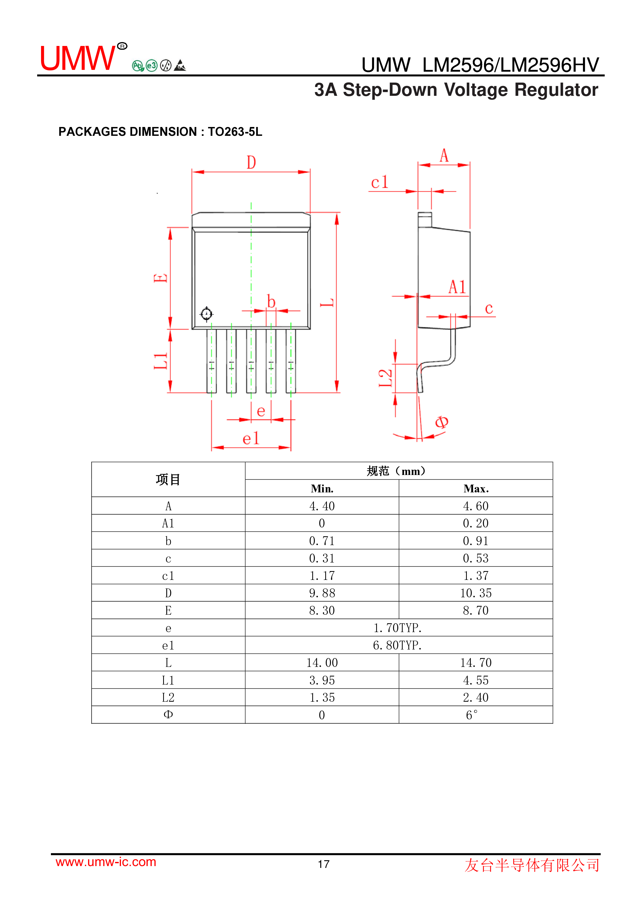
Package Information
- Package Type: TO-263-5 (D2PAK)
- Pin Count: 5 pins
- Mounting: SMD (Surface Mount Device)
- Thermal Pad: Large metal tab for heat dissipation
Pin Configuration
          LM2596S-ADJ (TO-263-5)
             Top View

        ┌───────────────────┐
        │   ▓▓▓▓▓▓▓▓▓▓▓▓▓   │ ← Thermal Tab (GND)
        │                   │
        │  1   2   3   4   5│
        └───┬───┬───┬───┬───┘
            │   │   │   │
           VIN OUT GND FB  ON/OFF
Pin Descriptions
| Pin | Name | Function |
|---|---|---|
| 1 | VIN | Voltage Input (4.5V - 40V) |
| 2 | OUTPUT | Switching Output (connect to inductor) |
| 3 | GND | Ground (also thermal tab) |
| 4 | FEEDBACK | Voltage Feedback Input (1.23V reference) |
| 5 | ON/OFF | Enable Control (Low or floating = ON; connection depends on topology - see ON/OFF Pin Configuration) |
| TAB | GND | Thermal Tab (must connect to GND plane) |
Application in This Project
In this project, three LM2596S-ADJ units are used in the following configuration:
U2: +15V → +13.5V Conversion (for +12V rail)
Key Points:
- Two-stage design: Buck converter (U2) reduces voltage with high efficiency, then linear regulator (LM7812) provides low-noise final output
- Capacitor order: C5/C6 (input filter) → [U2 + L1] → C3 (buck output filter) → [LM7812] → output capacitors
- C3 role: Filters switching ripple from buck converter before feeding the linear regulator
- Switching node: Junction at OUTPUT pin 2, where L1 and D1 cathode connect
- D1 flyback path: Provides current path when U2's internal switch is OFF (D1 cathode → switching node; D1 anode → GND)
- L1 output and D1 anode are completely separate paths - they do NOT connect to each other
View ASCII art circuit
Buck Converter IC: ┌──────────────────────┐ +15V IN ────────────┤1 VIN OUTPUT 2├─── Switching Node ──┬─→ L1 (100µH, 4.5A) ─→ +13.5V │ │ │ │ FB 4├─── Tap │ │ │ (feedback) │ ┌──┤3 GND │ │ │ │5 ON/OFF (tie to GND) │ D1 SS34 │ └──────────────────────┘ cathode GND LM2596S-ADJ │ (TO-263-5L) anode │ GND Input Capacitors (C6 closest to IC): +15V ──┬────────────────┬─── To IC Pin 1 │ │ C5 C6 100µF 100nF electrolytic ceramic (farther) (CLOSE!) │ │ GND GND Output Filter: ┌─── To Linear Regulator (LM7812) │ +13.5V ──────────┼─── C3 (470µF/25V) │ electrolytic │ │ │ GND │ Signal Path: +15V → [U2] → L1 → +13.5V → C3 → [LM7812] → +12V OUT Feedback Network (Voltage Divider with Compensation): +13.5V ──┬─── R1 (10kΩ) ───┬─── R2 (1kΩ) ─── GND │ │ └─── C31 (22nF) ──┤ │ Tap → To IC Pin 4 (FB) Components: - R1 (10kΩ) with C31 (22nF) in parallel: Creates pole-zero compensation (Type II) - R2 (1kΩ): Sets feedback tap voltage - C31 (22nF ceramic): Feedback compensation capacitor in parallel with R1 - Improves transient response and loop stability - Reduces switching noise on feedback line - Prevents oscillation Tap voltage = +13.5V × R2/(R1+R2) = 13.5V × 1kΩ/11kΩ = 1.23V U2 maintains FB pin at 1.23V reference by adjusting duty cycle
Output Voltage Calculation:
Vout = 1.23V × (1 + R1/R2)
     = 1.23V × (1 + 10kΩ/1kΩ)
     = 1.23V × 11
     = 13.53V
Component Values:
- L1: 100µH, 4.5A Inductor (JLCPCB: C19268674, CYA1265-100UH)
- D1: SS34 Schottky Diode 3A/40V (JLCPCB: C8678)
- C3: 470µF/25V Electrolytic Capacitor (JLCPCB: C3351)
- R1: 10kΩ ±1% 0603 (JLCPCB: C25804)
- R2: 1kΩ ±1% 0603 (JLCPCB: C21190)
- C4: 22nF Ceramic Capacitor (feedback compensation)
U3: +15V → +7.5V Conversion (for +5V rail)
+15V ─────┬─── L2: 100µH ──┬─── D2 ──┬─── C4: 470µF ──┬─→ +7.5V/0.6A
          │    (4.5A)      │   SS34  │    (10V)       │
          │                │    ↓    │                │
          │           ┌────┴─────────┴──┐             │
          │           │5  VIN      OUT │4────────────┤
          └───────────┤3  ON        FB │2─────┬──────┘
                      │1  GND          │      │
                      └────────────────┘      │
                              │               │
                             GND          ┌───┴───┐
                                          │ R3    │ 5.1kΩ
                                          │ 5.1kΩ │
                                          └───┬───┘
                                          ┌───┴───┐
                                          │ R4    │ 1kΩ
                                          │ 1kΩ   │
                                          └───┬───┘
                                              │
                                             GND
Output Voltage Calculation:
Vout = 1.23V × (1 + R3/R4)
     = 1.23V × (1 + 5.1kΩ/1kΩ)
     = 1.23V × 6.1
     = 7.50V
Component Values:
- L2: 100µH, 4.5A Inductor (JLCPCB: C19268674)
- D2: SS34 Schottky Diode (JLCPCB: C8678)
- C7: 470µF/25V Electrolytic Capacitor (JLCPCB: C3351)
- R3: 5.1kΩ ±1% 0603 (JLCPCB: C23186)
- R4: 1kΩ ±1% 0603 (JLCPCB: C21190)
- C32: 22nF Ceramic Capacitor (feedback compensation)
U4: -15V → -13.5V Conversion (for -12V rail)
-15V ─────┬─── L3: 100µH ──┬─── D3 ──┬─── C7: 470µF ──┬─→ -13.5V/0.9A
          │    (4.5A)      │   SS34  │    (25V)       │
          │                │    ↓    │                │
          │           ┌────┴─────────┴──┐             │
          │           │5  VIN      OUT │4────────────┤
          └───────────┤3  ON        FB │2─────┬──────┘
                      │1  GND          │      │
                      └────────────────┘      │
                              │               │
                             GND          ┌───┴───┐
                                          │ R5    │ 10kΩ
                                          │ 10kΩ  │
                                          └───┬───┘
                                          ┌───┴───┐
                                          │ R6    │ 1kΩ
                                          │ 1kΩ   │
                                          └───┬───┘
                                              │
                                             GND
Output Voltage: -13.53V (same calculation as U2)
Component Values:
- L3: 100µH, 4.5A Inductor (JLCPCB: C19268674)
- D3: SS34 Schottky Diode (JLCPCB: C8678)
- C11: 470µF/25V Electrolytic Capacitor (JLCPCB: C3351)
- R5: 10kΩ ±1% 0603 (JLCPCB: C25804)
- R6: 1kΩ ±1% 0603 (JLCPCB: C21190)
- C12: 22nF Ceramic Capacitor (feedback compensation)
Design Considerations
1. Feedback Resistor Selection
The output voltage is determined by the following formula:
Vout = Vref × (1 + R_upper / R_lower)
Where Vref = 1.23V (internal reference voltage).
Recommended Resistor Values:
- R_lower: 1kΩ (fixed, optimizes feedback current)
- R_upper: Select based on desired output voltage
| Target Vout | R_upper | Actual Vout |
|---|---|---|
| 3.3V | 1.7kΩ | 3.32V |
| 5V | 3.0kΩ | 4.92V |
| 7.5V | 5.1kΩ | 7.50V |
| 12V | 8.7kΩ | 12.01V |
| 13.5V | 10kΩ | 13.53V |
2. Feedback Compensation Network
All three buck converters in this project use a Type II compensation network consisting of a capacitor in parallel with the upper feedback resistor. This improves loop stability and transient response.
Topology:
Output ──┬─── R_upper ──┬─── R_lower ─── GND
         │              │
         └─── CFF ──────┤
                        │
                       Tap → To FB pin
Component Values:
- CFF (C4, C8, C12): 22nF ceramic capacitor
- In parallel with R_upper (R1, R3, R5)
Why 22nF for all three converters?
The compensation capacitor value depends on:
- Switching frequency (150kHz - same for all LM2596S units)
- LC filter characteristics (100µH inductor + 470µF output cap - same for all)
- Feedback resistor values (affect DC gain, but compensation pole/zero placement is similar)
Since all three converters use the same IC, switching frequency, inductor, and output capacitor, the same 22nF compensation value works optimally for all three circuits.
Benefits of CFF capacitor:
- Improves transient response during load changes
- Reduces switching noise on the feedback line
- Prevents control loop oscillation
- Creates a pole-zero pair for Type II compensation
Reference: See LM2596 datasheet Figure 1 (page 9) for the compensation capacitor (CFF) in the typical application circuit.
3. Inductor Selection
Key Parameters:
- Inductance: 100µH (recommended, selectable within 47µH-220µH range)
- Saturation Current: 1.5x or more of output current (4.5A or higher for this project)
- DCR (DC Resistance): As low as possible (for improved efficiency)
Selected Component for This Project:
- CYA1265-100UH: 100µH, 4.5A saturation current, SMD power inductor
- JLCPCB: C19268674
4. Diode Selection
Schottky Diode Required:
- High-speed switching capability (150kHz)
- Low forward voltage drop (for improved efficiency)
- Current Rating: Equal to or greater than output current (3A for this project)
- Reverse Voltage: Equal to or greater than input voltage (40V or higher recommended)
Selected Component for This Project:
- SS34: 3A, 40V Schottky Diode
- JLCPCB: C8678 (Very High Stock: 1,859,655 units)
5. Capacitor Selection
Input Capacitor (Between VIN and GND):
- Electrolytic or ceramic capacitor
- Capacitance: 100µF or higher recommended
- Voltage Rating: 1.5x or more of input voltage
Output Capacitor (Between VOUT and GND):
- Required: Low ESR electrolytic capacitor
- Capacitance: 220µF - 1000µF (470µF for this project)
- ESR: 0.5Ω or less (for ripple reduction)
- Voltage Rating: 1.5x or more of output voltage
6. PCB Layout Guidelines
Important Points:
- Input loop: Minimize the area of VIN - L - D - Cout loop
- Ground plane: Ensure a continuous, wide GND plane
- Thermal relief: Connect TO-263 package tab directly to GND plane
- FB trace: Keep feedback trace short and away from noise sources
- Via placement: Place multiple thermal vias (for enhanced heat dissipation)
Recommended Trace Widths:
- VIN, VOUT: 2mm or wider (for 3A current handling)
- GND: As wide as possible (plane recommended)
- FB: 0.2mm-0.3mm (thin and short)
7. Efficiency Optimization
Factors Affecting Efficiency:
- Inductor DCR: Lower is better
- Diode Vf: Lower is better (Schottky recommended)
- Output capacitor ESR: Lower is better
- Input-Output voltage difference: Smaller difference yields higher efficiency
Efficiency Estimates for This Project:
- U2 (15V→13.5V): ~88% (High efficiency due to small voltage difference)
- U3 (15V→7.5V): ~85% (Moderate voltage difference)
- U4 (-15V→-13.5V): ~88% (Equivalent efficiency for negative voltage)
8. ON/OFF Pin Configuration
The ON/OFF pin (pin 5) behavior differs between regular buck converters and inverting buck-boost configurations due to the bootstrapped ground reference.
Regular Buck Configuration (U2, U3)
Connection: ON pin tied to system GND (0V) or left floating
U2, U3 (Buck Converters):
Pin 5 (ON/OFF) ──→ System GND (0V)
Pin 3 (IC GND)  ──→ System GND (0V)
How it works:
- IC GND pin is at system ground (0V)
- ON/OFF threshold: <1.3V above IC GND = <1.3V system reference
- Tying to system GND (0V) = LOW = ENABLED ✅
- Pulling >1.6V = HIGH = DISABLED
Inverting Buck-Boost Configuration (U4)
Connection: ON pin tied to IC GND (-13.5V) or left floating
U4 (Inverting Buck-Boost):
Pin 5 (ON/OFF) ──→ IC GND (-13.5V) [connected to pin 3]
Pin 3 (IC GND)  ──→ -13.5V output (bootstrapped)
Critical difference:
- IC GND pin is at -13.5V (bootstrapped to negative output), NOT system ground
- ON/OFF threshold: <1.3V above IC GND = <-12.2V system reference
- Cannot connect to system GND (0V) - this would be +13.5V above IC GND = DISABLED ❌
- Must connect to IC GND (-13.5V) or leave floating = ENABLED ✅
Comparison Table
| Topology | IC GND Location | ON Pin Connection | Enable Voltage | Disable Voltage |
|---|---|---|---|---|
| U2, U3 (Buck) | System GND (0V) | System GND or float | <1.3V (system ref) | >1.6V (system ref) |
| U4 (Inverting) | -13.5V output | IC GND or float | <-12.2V (system ref) | >-11.9V (system ref) |
Why This Matters
For always-on operation (this project):
- U2, U3: Tie ON pin to system GND (explicit, better noise immunity)
- U4: Tie ON pin to IC GND (pin 3, at -13.5V) - shown in Diagram4
For shutdown control (not used in this project):
- U2, U3: Simple - pull pin above 1.6V (system ground referenced)
- U4: Complex - requires optocoupler or level-shifter (see TI app note SNVA722B)
Internal Pull-Down Behavior
The LM2596S has an internal pull-down resistor on the ON/OFF pin:
- Pulls the pin toward IC GND (wherever IC GND is connected)
- Keeps pin LOW relative to IC GND when floating
- Result: Floating = ENABLED for both topologies
Best practice: Explicitly connect to IC GND rather than relying on internal pull-down for better noise immunity.
9. Thermal Considerations
Heat Dissipation Calculation Example (U2: 15V→13.5V, 1.3A):
Output power:    P_out = V_out × I_out = 13.5V × 1.3A = 17.55W
Input power:     P_in = P_out / Efficiency = 17.55W / 0.88 = 19.94W
Power dissipation: P_diss = P_in - P_out = 19.94W - 17.55W = 2.39W

Alternative formula for switching regulators:
P_diss = P_out × ((1 - η) / η) = 17.55W × (0.12 / 0.88) = 2.39W
TO-263 package thermal resistance: ~40°C/W (without thermal vias), ~25°C/W (with thermal vias)
Without thermal vias:
- Temperature rise: 2.39W × 40°C/W = 95.6°C
- Junction temp (25°C ambient): 25°C + 95.6°C = 120.6°C ⚠️
- WARNING: Approaches maximum operating temperature (125°C)
With thermal vias (recommended):
- Temperature rise: 2.39W × 25°C/W = 59.8°C
- Junction temp (25°C ambient): 25°C + 59.8°C = 84.8°C ✅
- Safe margin: 40°C below maximum temperature
Conclusion: Thermal vias are REQUIRED under TO-263 thermal pad for reliable operation at full load
JLCPCB Information
- Part Number: C347423
- Manufacturer P/N: LM2596S-ADJ(UMW)
- Manufacturer: UMW (Youtai Semiconductor)
- Stock Availability: 12,075 units
- Package: TO-263-5
- Price: $0.266 (as of December 2024)
Note: The UMW version is a compatible replacement for the Texas Instruments LM2596S-ADJ. Electrical characteristics are equivalent, and the price is significantly lower.
External Resources
- JLCPCB Part Page - Official part page
- Texas Instruments LM2596 Datasheet - Original datasheet
- SIMPLE SWITCHER Design Tools - TI official design tools
Notes
- The LM2596S-ADJ is a very common DC-DC converter, and many compatible parts exist
- The 150kHz switching frequency avoids audible noise (below 20kHz)
- ON/OFF pin connection differs between regular buck (U2, U3) and inverting buck-boost (U4) - see ON/OFF Pin Configuration for details
- This project uses the always-on configuration for all three converters
- Feedback resistors with ±1% tolerance are recommended (directly affects output voltage accuracy)