L7805ABD2T-TR - +5V Linear Regulator
Fixed positive voltage regulator providing stable +5V output in compact TO-263-2 (D2PAK) surface-mount package with excellent thermal performance.

Overview
The L7805ABD2T-TR is a three-terminal positive voltage regulator in TO-263-2 (D2PAK) package, designed to provide a fixed +5V output from a higher input voltage. This component serves as the final stage in the +5V power rail, converting the +7.5V DC-DC output to a clean, low-noise +5V suitable for modular synthesizer digital circuits and control voltage applications.
Key Specifications
| Parameter | Value | Notes |
|---|---|---|
| JLCPCB Part Number | C86206 | |
| Manufacturer Part Number | L7805ABD2T-TR | |
| Package | TO-263-2 (D2PAK) | Surface-mount |
| Stock Availability | 272,379 units | Very high availability |
| Unit Price | $0.11 | JLCPCB pricing |
| Output Voltage | 5V ±4% | 4.8V - 5.2V |
| Output Current | 1.5A max | Design uses 0.5A |
| Dropout Voltage | ~2V typical | Minimum VIN = 7V |
| Line Regulation | ±0.5% typical | Input voltage variation |
| Load Regulation | ±1% typical | Output current variation |
| Ripple Rejection | >60dB | @120Hz |
| Quiescent Current | ~5mA typical | No-load consumption |
| Thermal Resistance θJC | 3°C/W | Junction to case (tab) |
| Thermal Resistance θJA | 35°C/W | Junction to ambient |
| Operating Temp Range | 0°C to +125°C | Junction temperature |
Pin Configuration
         TO-263-2 (D2PAK) Package
              Top View

         ┌──────────────┐
         │              │
         │   L7805A     │
         │   BD2T-TR    │
         │              │
         │              │
         └──┬───────┬───┘
            │       │
          PIN1    PIN2
          INPUT    GND
         (+7.5V) (Common)

              TAB
           (OUTPUT)
            (+5V)

         Side View

         ┌──────────────┐
         │   Component  │ ← Surface mount IC
         └──┬───────┬───┘
            │       │
          PIN1    PIN2

    ════════════════════  ← Metal tab (OUTPUT)
                            soldered to PCB pad
Pin Descriptions
| Pin | Name | Function | Connection in Design |
|---|---|---|---|
| 1 | INPUT | Unregulated input voltage | +7.5V from DC-DC converter (U3) |
| 2 | GND | Ground reference (common) | System ground plane |
| TAB | OUTPUT | Regulated +5V output (metal tab) | +5V rail with protection circuit |
Note: Unlike TO-220 package, the TO-263-2 has the OUTPUT on the metal tab, not on pin 3.
Application Circuit
+7.5V (from DC-DC) ───┬─── C12: 470nF ───┬─── U7: L7805ABD2T ───┬─── C15: 100nF ───┬─→ +5V OUT
                      │                  │                      │                  │
                      │                  │    ┌──────────┐      │                  │
                      │                  └────│1  INPUT  │      │                  │
                      │                       │          │      │                  │
                      │                    ┌──│2   GND   │      │                  │
                      │                    │  │          │      │                  │
                      │                    │  │   TAB ───┴──────┴──────────────────┤
                      │                    │  └──────────┘                         │
                      │                    │     (OUTPUT)                          │
                      └─── C19: 470µF ─────┼─────────┬─── C20: 470µF ──────────────┤
                           (Input)         │         │    (Output)                 │
                                           │         │                             │
                                          GND       GND                            │
                                                                                   │
                                        ┌──────────────────────────────────────────┘
                                        │
                                  ┌─────┴─────┐
                                  │   LED3    │ Blue Status LED
                                  │  (Blue)   │ via R8: 1kΩ
                                  └─────┬─────┘
                                        │
                                       GND
Component Values
Input Capacitors
| Reference | Value | Type | Voltage | Package | Part Number | Purpose |
|---|---|---|---|---|---|---|
| C12 | 470nF | Ceramic X7R | 25V | 0603 | C1623 | High-frequency noise filtering |
| C19 | 470µF | Electrolytic | 10V | D6.3xL7.7mm | C335982 | Input voltage stabilization |
Output Capacitors
| Reference | Value | Type | Voltage | Package | Part Number | Purpose |
|---|---|---|---|---|---|---|
| C15 | 100nF | Ceramic X7R | 50V | 0805 | C49678 | High-frequency decoupling |
| C20 | 470µF | Electrolytic | 10V | D6.3xL7.7mm | C335982 | Load transient response |
Status LED Circuit
| Reference | Part | Value | Package | Part Number | Purpose |
|---|---|---|---|---|---|
| LED3 | Blue LED | 2.8V @ 10mA | 0805 | C72041 | Power status indicator |
| R8 | Resistor | 1kΩ | 0603 | C21190 | LED current limiting |
Design Considerations
Input Voltage Requirements
The L7805ABD2T requires a minimum input voltage of approximately 7V for proper regulation (5V output + 2V dropout). In this design:
- Input voltage: +7.5V from LM2596S DC-DC converter
- Dropout margin: 7.5V - 5V = 2.5V
- Status: ✅ Excellent - well above minimum dropout voltage
The 2.5V margin provides:
- Stable regulation across load variations
- Tolerance for input voltage ripple
- Reduced power dissipation compared to higher input voltages
- Optimal efficiency for the linear regulator stage
Thermal Management
Power dissipation calculation:
P = (VIN - VOUT) × IOUT
P = (7.5V - 5V) × 0.5A
P = 2.5V × 0.5A
P = 1.25W
Temperature rise without additional heatsinking:
ΔT = P × θJA
ΔT = 1.25W × 35°C/W
ΔT = 43.75°C
At 25°C ambient, junction temperature = 68.75°C (well within 125°C maximum).
Thermal performance advantages of TO-263-2:
- Lower θJA than TO-220 (35°C/W vs 50°C/W)
- Large metal tab provides excellent heat spreading
- Direct thermal contact with PCB copper pour
- No additional heatsink required for this application
PCB copper area recommendations:
- Minimum: 2 cm² copper pour connected to tab
- Recommended: 5 cm² copper pour for better margin
- Thermal vias: 6-10 vias (0.3mm) under tab to bottom layer
Capacitor Placement
Critical for stability and noise rejection:
- C12 (470nF ceramic): Place within 5mm of pin 1
- Purpose: Suppress high-frequency noise from DC-DC stage
- Type: X7R or better (maintains capacitance vs. temperature)
- C19 (470µF electrolytic): Place within 10mm of pin 1
- Purpose: Stabilize input voltage during load transients
- Polarity: Positive terminal to input, negative to ground
- C15 (100nF ceramic): Place within 5mm of output tab
- Purpose: High-frequency output decoupling
- Critical for preventing oscillation
- Must be ceramic for low ESR/ESL
- C20 (470µF electrolytic): Place within 10mm of output tab
- Purpose: Improve load transient response
- ESR: <2Ω for best performance
- Helps with sudden current demands
Ground Plane Connection
The TO-263-2 package requires careful PCB layout:
- Pin 2 (GND): Connect directly to ground plane with wide trace
- Tab (OUTPUT): Large copper pour for both electrical and thermal connection
- Thermal vias: Essential for heat dissipation to inner/bottom layers
- Keep-out area: Maintain clearance around pins for solder inspection
Performance Characteristics
Regulation Performance
| Condition | Specification | Typical Performance |
|---|---|---|
| Line regulation | VIN = 7V to 25V | ±0.5% (±25mV) |
| Load regulation | IOUT = 5mA to 1.5A | ±1% (±50mV) |
| Output voltage accuracy | At 25°C | ±4% (±200mV) |
| Temperature coefficient | -40°C to +125°C | ±1mV/°C typical |
Noise Performance
| Parameter | Value | Conditions |
|---|---|---|
| Ripple rejection | 60dB min | f = 120Hz |
| Output noise voltage | <1mVp-p | With recommended capacitors |
| Transient response | <50µs | 250mA load step |
| PSRR (Power Supply Rejection) | >60dB | 100Hz - 10kHz |
Protection Features
Built-in Protections
- Thermal Shutdown: Automatically shuts down if junction temperature exceeds 150°C
- Short Circuit Protection: Current limiting prevents damage during output short
- Safe Operating Area (SOA): Internal circuitry ensures operation within safe limits
- Reverse Polarity: Input diode protects against reverse voltage
External Protection (This Design)
+5V (from U7) ───┬─── PTC2: 1.1A ───┬─── F2: 1.5A ──┬─── TVS2: SD05 ────────┬─→ +5V OUT
                 │  (Auto-Reset)    │   (Backup)    │   (5V Clamp)          │
                 │                  │               │      ↕                │
                 │                  │               └─────GND────────────────┤
                 │                  │                                       │
                 └─── LED3 (Blue) via R8 (1kΩ) ──────────────→ Power Status
Protection stages:
- Overload (0.6A-1.5A): PTC2 trips → Auto-reset after cooling
- Short circuit (>1.5A): F2 blows → Manual replacement required
- Overvoltage: TVS2 clamps transients above 6V (unidirectional)
Note: The TVS2 (SD05) is unidirectional, optimized for positive DC power rail protection.
Bill of Materials
| Designator | Part | Value | Package | JLCPCB Part # | Qty | Unit Price | Extended |
|---|---|---|---|---|---|---|---|
| U7 | L7805ABD2T-TR | Fixed +5V LDO | TO-263-2 | C86206 | 1 | $0.11 | $0.11 |
| C12 | Ceramic Cap | 470nF 25V X7R | 0603 | C1623 | 1 | $0.0036 | $0.0036 |
| C15 | Ceramic Cap | 100nF 50V X7R | 0805 | C49678 | 1 | $0.0021 | $0.0021 |
| C19, C20 | Electrolytic | 470µF 10V | D6.3xL7.7mm | C335982 | 2 | $0.014 | $0.028 |
| LED3 | LED | Blue 0805 | 0805 | C72041 | 1 | $0.0126 | $0.0126 |
| R8 | Resistor | 1kΩ ±1% | 0603 | C21190 | 1 | $0.0005 | $0.0005 |
| Total | $0.16 |
Alternative Parts
Direct Replacements (TO-263-2 Package)
| Part Number | Manufacturer | JLCPCB Part # | Stock | Price | Notes |
|---|---|---|---|---|---|
| L7805ABD2T-TR | STMicroelectronics | C86206 | 272,379 | $0.11 | Recommended (very high stock) |
| MC7805BD2T | ON Semiconductor | Check | Check | ~$0.12 | Pin-compatible |
| UA7805CKC | Texas Instruments | Check | Check | ~$0.13 | Pin-compatible |
Package Alternatives
| Package | Part Number | JLCPCB Part # | Stock | Price | Notes |
|---|---|---|---|---|---|
| TO-263-2 | L7805ABD2T-TR | C86206 | 272,379 | $0.11 | Recommended (best thermal) |
| TO-220 | L7805CV | C2846 | 55,629 | $0.11 | Through-hole alternative |
| SOT-89 | AMS1117-5.0 | C6187 | High | $0.05 | Lower current (1A max) |
Recommendation: Stick with TO-263-2 for SMD assembly and superior thermal performance.
PCB Layout Guidelines
Footprint Requirements
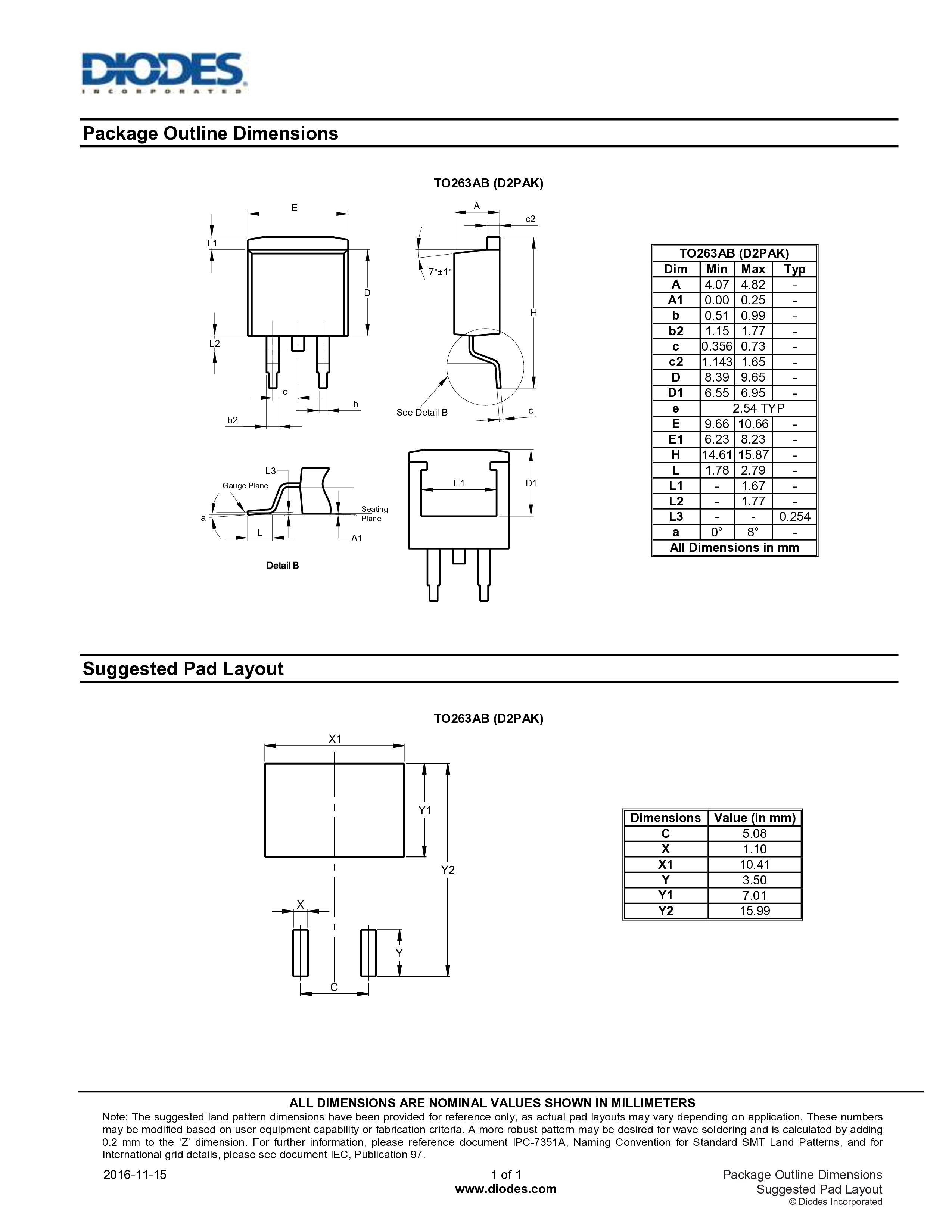
TO-263-2 (D2PAK) package footprint specifications:
         Top View (PCB Pad Layout)

    ┌──────────────────────────────┐
    │                              │
    │    Large Copper Pour         │  ← OUTPUT TAB
    │    (5cm² recommended)        │     thermal + electrical
    │                              │
    │         Thermal Vias         │
    │         (6-10 vias)          │
    │                              │
    └──────────────────────────────┘

         PIN1 ■        PIN2 ■
        (INPUT)        (GND)

    Pin spacing: 2.54mm (0.1")
    Pin pad: 1.5mm x 2.0mm
    Tab pad: 10mm x 10mm (minimum)
            15mm x 15mm (recommended)
Recommended Pad Dimensions
| Pad | Width | Length | Purpose |
|---|---|---|---|
| Pin 1 (INPUT) | 1.5mm | 2.0mm | Solder pad for input pin |
| Pin 2 (GND) | 2.0mm | 3.0mm | Larger for ground connection |
| Tab (OUTPUT) | 10-15mm | 10-15mm | Thermal and electrical connection |
Layout Recommendations
- Component placement:
- Orient IC with tab facing interior of PCB (away from edge)
- Maximize copper area under and around tab
- Keep input and output capacitors on same side as regulator
- Copper pours:
- Create large copper pour (5cm² minimum) connected to output tab
- Top layer: Main output pad and distribution
- Bottom layer: Additional copper connected via thermal vias
- Inner layers (4-layer board): Additional ground/power planes
- Thermal vias:
- Place 6-10 thermal vias (0.3mm diameter) under tab
- Arrange in grid pattern for even heat distribution
- Connect to bottom layer copper pour
- Do NOT use thermal relief on these vias (direct connection needed)
- Via spacing: ~2mm apart
- Trace widths:
- Input trace (7.5V): 0.5mm minimum (0.5A current, low voltage drop)
- Output trace (5V): 1mm minimum (0.5A current)
- Ground: Maximum copper pour area
- High-current paths: 2mm or copper pour preferred
-
Capacitor placement:
C12 ──┐  ┌── IC ──┐  ┌── C15
      │  │        │  │
C19 ──┘  │  U7    │  └── C20
         │        │
         └────────┘

Distance:
- C12: <5mm from pin 1
- C19: <10mm from pin 1
- C15: <5mm from output tab
- C20: <10mm from output tab
Thermal Via Pattern
    Recommended thermal via pattern
    under TO-263-2 tab:

    ┌─────────────────────────┐
    │  ●    ●    ●    ●    ●  │
    │                         │
    │  ●    ●    ●    ●    ●  │  ← 0.3mm vias
    │                         │     2mm spacing
    │  ●    ●    ●    ●    ●  │
    │                         │
    └─────────────────────────┘

    Total vias: 15 (aggressive cooling)
    Minimum: 6 vias
    Recommended: 10 vias
Assembly Considerations
Soldering Guidelines
Reflow soldering (recommended for production):
- Peak temperature: 260°C maximum
- Time above 220°C: 60-90 seconds
- Solder paste: SAC305 or similar lead-free
- Stencil thickness: 0.125mm (5 mil)
Hand soldering:
- Soldering iron: 350°C maximum
- Solder pin 1 and pin 2 first
- Apply solder to tab from component side
- Ensure good thermal contact between tab and PCB pad
- Use generous solder for tab connection
Inspection Points
After assembly, inspect:
- Pin solder joints: Smooth fillet, no bridges
- Tab solder joint: Good coverage, no voids visible
- Component alignment: Centered on pads
- No cold solder joints: Shiny, smooth finish
- Thermal via filling: Solder should wick into vias
Testing and Validation
Input Voltage Test
- Apply 7.5V to input with no load
- Verify output voltage: 4.8V - 5.2V (5V ±4%)
- Measure quiescent current: <10mA
Load Regulation Test
- Connect variable load (0-1.0A)
- Measure output voltage at different load currents:
- 0mA: Should be within 5V ±2%
- 250mA: Should be within 5V ±3%
- 500mA: Should be within 5V ±4%
- Verify voltage drop <50mV from no-load to full-load
Thermal Test
- Apply 0.5A load for 30 minutes
- Measure case temperature with thermal camera or thermocouple
- Verify case temperature <70°C at 25°C ambient
- Compare to calculation: Should be ~69°C
- Check for thermal shutdown (should not occur)
Ripple and Noise Test
- Connect oscilloscope (AC coupling, 20MHz bandwidth limit)
- Use short ground lead or coax probe
- Measure output with 0.5A load
- Verify peak-to-peak ripple <5mVp-p (target: <1mVp-p)
- Check for oscillation or instability (should be stable)
Transient Response Test
- Use electronic load with step function (0A → 0.5A)
- Monitor output voltage on oscilloscope
- Verify voltage dip <250mV during load step
- Verify recovery time <100µs
- Check for ringing or overshoot
Troubleshooting
| Symptom | Possible Cause | Solution |
|---|---|---|
| No output voltage | Input voltage too low | Verify 7.5V input from DC-DC |
| Shorted output | Check for shorts on +5V rail | |
| Thermal shutdown | Reduce load, check thermal vias | |
| Poor tab solder joint | Reflow tab solder connection | |
| Low output voltage | Insufficient input voltage | Check DC-DC stage output (should be 7.5V) |
| Excessive load current | Verify load <0.5A (design spec) | |
| Poor ground connection | Check pin 2 and ground plane | |
| High trace resistance | Check trace widths and connections | |
| High ripple noise | Missing input capacitor | Verify C12, C19 installed correctly |
| Missing output capacitor | Verify C15, C20 installed correctly | |
| Poor capacitor placement | Move capacitors closer to IC | |
| Ground loop issues | Check ground plane continuity | |
| Oscillation | Missing C15 (100nF output) | Add C15 close to output tab |
| Long output traces | Shorten traces, add local decoupling | |
| Capacitive load | Add series resistance (1Ω) at output | |
| Poor ground routing | Improve ground plane connections | |
| Overheating | Excessive power dissipation | Check input voltage (should be 7.5V) |
| Insufficient copper area | Increase copper pour under tab | |
| No thermal vias | Add thermal vias under tab | |
| Poor thermal contact | Check solder joint on tab | |
| Voltage too high | Wrong regulator installed | Verify L7805A not L7812 or other |
| Open feedback loop | Check internal IC (unlikely) | |
| Voltage too low | Input voltage marginal | Verify 7.5V input stable |
| Excessive load | Reduce load current |
Application Notes
Digital vs. Analog Loads
The +5V rail in modular synthesizers may power:
Digital circuits (microcontrollers, logic ICs):
- Characteristics: Switching loads, transient currents
- Decoupling: Add 100nF ceramic capacitor at each IC
- Distribution: Star topology from main filter cap
Analog circuits (op-amps, comparators):
- Characteristics: Steady loads, noise-sensitive
- Decoupling: 100nF ceramic + 10µF electrolytic per section
- Isolation: Consider RC filter if needed (10Ω + 100µF)
Low-Noise Operation
For ultra-low-noise applications:
- Additional output filtering:
- Add 10Ω resistor + 100µF capacitor LC filter
- Creates additional pole at ~160Hz
- Reduces high-frequency noise
- Separate analog/digital grounds:
- Split +5V distribution into analog and digital sections
- Join grounds at single star point
- Prevents digital switching noise coupling
- Shielding:
- Route +5V traces away from high-frequency signals
- Use ground plane as shield
- Keep sensitive analog circuits away from digital sections
Related Components
- Upstream: LM2596S-ADJ #2 (U3) - Provides +7.5V input
- Downstream: Protection circuit (PTC2, F2, TVS2)
- Parallel regulators: L7812CV-DG (U6), CJ7912 (U8)
References
- L7805ABD2T-TR Datasheet - STMicroelectronics
- JLCPCB Part C86206
- TO-263 Package Thermal Design
- Related documentation: Diagram6 - +5V Linear Regulator