CJ7912 - -12V Negative Linear Regulator
Fixed negative voltage regulator providing stable -12V output in compact TO-252-2L (DPAK) surface-mount package for negative power rail applications.

Overview
The CJ7912 is a three-terminal negative voltage regulator in TO-252-2L (DPAK) package, designed to provide a fixed -12V output from a more negative input voltage. This component serves as the final stage in the -12V power rail, converting the -13.5V DC-DC output to a clean, low-noise -12V suitable for modular synthesizer op-amp circuits and analog signal processing.
Key Specifications
| Parameter | Value | Notes |
|---|---|---|
| JLCPCB Part Number | C94173 | |
| Manufacturer Part Number | CJ7912 | |
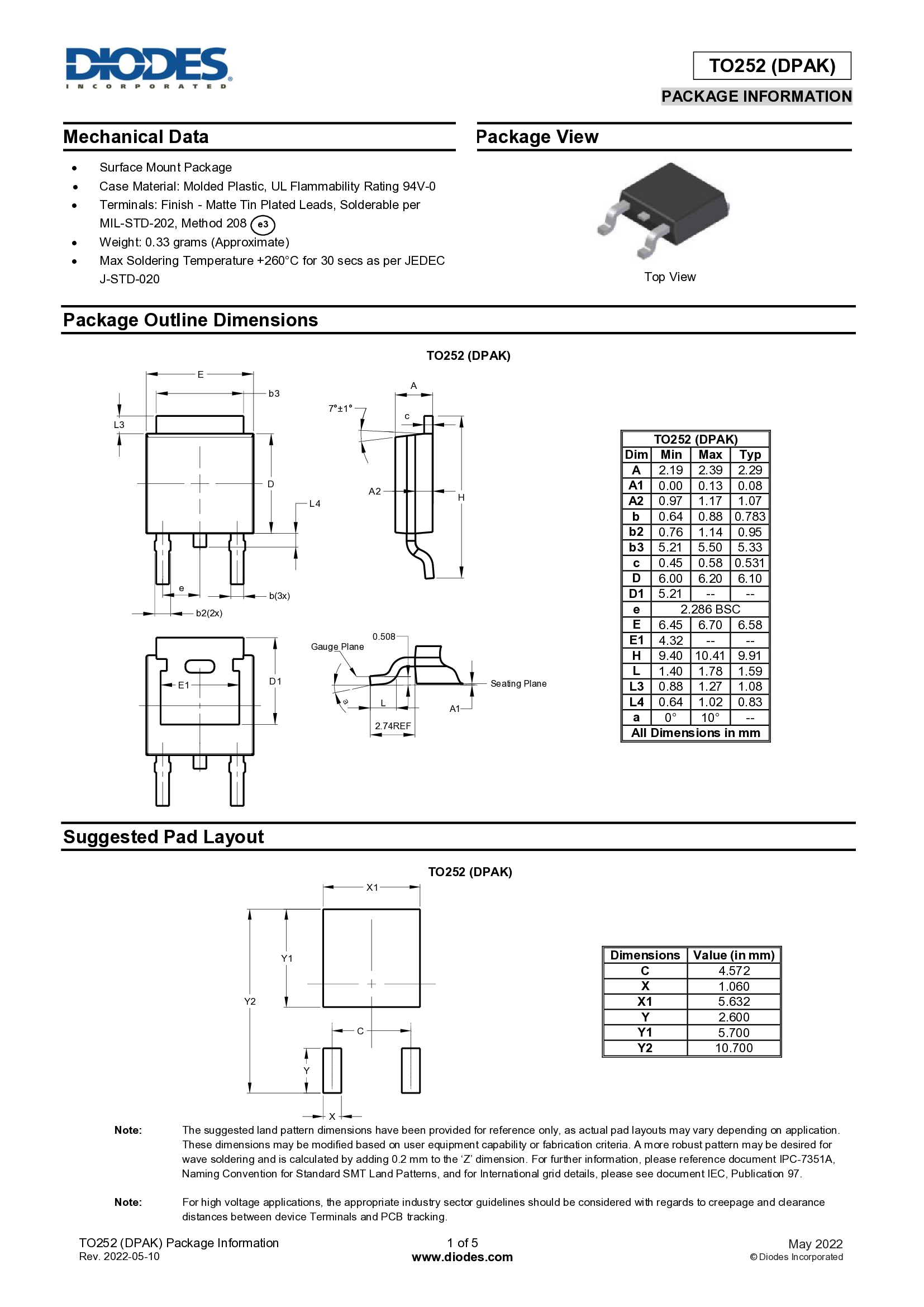
| Package | TO-252-2L (DPAK) | Surface-mount |
| Stock Availability | 15,466 units | Moderate availability |
| Unit Price | $0.11 | JLCPCB pricing |
| Output Voltage | -12V ±4% | -11.52V to -12.48V |
| Output Current | 1.5A max | Design uses 0.8A |
| Dropout Voltage | ~2V typical | Maximum VIN = -14V |
| Line Regulation | ±0.5% typical | Input voltage variation |
| Load Regulation | ±1% typical | Output current variation |
| Ripple Rejection | >60dB | @120Hz |
| Quiescent Current | ~5mA typical | No-load consumption |
| Thermal Resistance θJC | 5°C/W | Junction to case (tab) |
| Thermal Resistance θJA | 40°C/W | Junction to ambient |
| Operating Temp Range | 0°C to +125°C | Junction temperature |
Pin Configuration
         TO-252-2L (DPAK) Package
              Top View

         ┌──────────────┐
         │              │
         │    CJ7912    │
         │              │
         │              │
         │              │
         └──┬───────┬───┘
            │       │
          PIN1    PIN2
           GND    INPUT
        (Common) (-13.5V)

              TAB
           (OUTPUT)
            (-12V)

         Side View

         ┌──────────────┐
         │   Component  │ ← Surface mount IC
         └──┬───────┬───┘
            │       │
          PIN1    PIN2

    ════════════════════  ← Metal tab (OUTPUT)
                            soldered to PCB pad
Pin Descriptions
| Pin | Name | Function | Connection in Design |
|---|---|---|---|
| 1 | GND | Ground reference (common) | System ground plane |
| 2 | INPUT | Unregulated input voltage | -13.5V from DC-DC converter (U4) |
| TAB | OUTPUT | Regulated -12V output (metal tab) | -12V rail with protection circuit |
Critical Note: This is a NEGATIVE voltage regulator. Pin numbering and voltage polarities are different from positive regulators:
- Pin 1 is GND (not INPUT like 78xx series)
- Pin 2 is INPUT (not GND like 78xx series)
- More negative voltage is "higher" voltage for this regulator
- Input must be more negative than output (-13.5V is "higher" than -12V)
Application Circuit
-13.5V (from DC-DC) ──┬─── C13: 470nF ───┬─── U8: CJ7912 ────┬─── C16: 100nF ───┬─→ -12V OUT
                      │                  │                   │                  │
                      │                  │    ┌──────────┐   │                  │
                      │                  └────│2  INPUT  │   │                  │
                      │                       │          │   │                  │
                      │                    ┌──│1   GND   │   │                  │
                      │                    │  │          │   │                  │
                      │                    │  │   TAB ───┴───┴──────────────────┤
                      │                    │  └──────────┘                      │
                      │                    │     (OUTPUT)                       │
                      └─── C21: 470µF ─────┼─────────┬─── C22: 470µF ───────────┤
                           (Input)         │         │    (Output)              │
                                           │         │                          │
                                          GND       GND                         │
                                                                                │
                                        ┌───────────────────────────────────────┘
                                        │
                                  ┌─────┴─────┐
                                  │   LED4    │ Red Status LED
                                  │   (Red)   │ via R9: 1kΩ
                                  └─────┬─────┘
                                        │
                                       GND
Component Values
Input Capacitors
| Reference | Value | Type | Voltage | Package | Part Number | Purpose |
|---|---|---|---|---|---|---|
| C13 | 470nF | Ceramic X7R | 25V | 0603 | C1623 | High-frequency noise filtering |
| C21 | 470µF | Electrolytic | 25V | D10xL10.2mm | C3351 | Input voltage stabilization |
Important: For C21, negative terminal connects to -13.5V input, positive terminal connects to GND.
Output Capacitors
| Reference | Value | Type | Voltage | Package | Part Number | Purpose |
|---|---|---|---|---|---|---|
| C16 | 100nF | Ceramic X7R | 50V | 0805 | C49678 | High-frequency decoupling |
| C22 | 470µF | Electrolytic | 25V | D10xL10.2mm | C3351 | Load transient response |
Important: For C22, negative terminal connects to -12V output, positive terminal connects to GND.
Status LED Circuit
| Reference | Part | Value | Package | Part Number | Purpose |
|---|---|---|---|---|---|
| LED4 | Red LED | 2.0V @ 10mA | 0805 | C84256 | Power status indicator |
| R9 | Resistor | 1kΩ | 0603 | C21190 | LED current limiting |
LED Connection: Anode to GND, Cathode to -12V through R9 (reverse of positive rail LEDs).
Design Considerations
Negative Voltage Concepts
Understanding negative voltage regulators:
Voltage Levels (relative to GND = 0V):

                GND (0V) ─────────────────
                  │
                  │ +13.5V "above" ground
                  │
              +13.5V ─────────────────

                GND (0V) ─────────────────
                  │
                  │ 12V "below" ground
                  │
              -12V ─────────────────
                  │
                  │ 13.5V "below" ground
                  │
              -13.5V ─────────────────

For negative regulator:
- INPUT = -13.5V (more negative)
- OUTPUT = -12V (less negative)
- Dropout = |VIN| - |VOUT| = 13.5V - 12V = 1.5V
Input Voltage Requirements
The CJ7912 requires input voltage to be at least 2V more negative than the output for proper regulation:
- Input voltage: -13.5V from LM2596S DC-DC converter
- Output voltage: -12V
- Dropout margin: 13.5V - 12V = 1.5V
- Status: ⚠️ Marginal - operates near minimum dropout voltage
The 1.5V margin is slightly below the typical 2V dropout specification but acceptable because:
- The DC-DC stage is regulated at -13.5V
- The CJ7912 can regulate with 1.5V dropout at lower currents
- Actual load current (0.8A) is well below maximum rating (1.5A)
- Negative regulators often have slightly lower dropout than positive equivalents
Recommendation: For production, consider increasing DC-DC output to -14.0V for better dropout margin.
Thermal Management
Power dissipation calculation:
P = (|VIN| - |VOUT|) × IOUT
P = (13.5V - 12V) × 0.8A
P = 1.5V × 0.8A
P = 1.2W
Temperature rise without additional heatsinking:
ΔT = P × θJA
ΔT = 1.2W × 40°C/W
ΔT = 48°C
At 25°C ambient, junction temperature = 73°C (well within 125°C maximum).
Thermal performance of TO-252-2L:
- Moderate θJA (40°C/W)
- Metal tab provides good heat spreading
- Direct thermal contact with PCB copper pour
- No additional heatsink required for this application
PCB copper area recommendations:
- Minimum: 3 cm² copper pour connected to tab
- Recommended: 6 cm² copper pour for better margin
- Thermal vias: 6-8 vias (0.3mm) under tab to bottom layer
Capacitor Placement and Polarity
Critical for negative regulators: Electrolytic capacitor polarity is REVERSED from what you might expect:
Correct polarity for negative rail:

C21 (Input, 470µF):
         ┌─────────┐
  GND ───┤+       -├─── -13.5V
         └─────────┘

C22 (Output, 470µF):
         ┌─────────┐
  GND ───┤+       -├─── -12V
         └─────────┘

REMEMBER:
- Positive terminal goes to GROUND (0V)
- Negative terminal goes to negative voltage
- This is OPPOSITE of positive voltage regulators
Placement guidelines:
- C13 (470nF ceramic): Place within 5mm of pin 2
- Purpose: Suppress high-frequency noise from DC-DC stage
- Non-polarized, so no polarity concerns
- C21 (470µF electrolytic): Place within 10mm of pin 2
- Purpose: Stabilize input voltage during load transients
- POLARITY: + to GND, - to -13.5V
- C16 (100nF ceramic): Place within 5mm of output tab
- Purpose: High-frequency output decoupling
- Critical for preventing oscillation
- C22 (470µF electrolytic): Place within 10mm of output tab
- Purpose: Improve load transient response
- POLARITY: + to GND, - to -12V
Ground Plane Connection
The TO-252-2L package layout:
- Pin 1 (GND): Wide connection directly to ground plane
- Pin 2 (INPUT): Connect to -13.5V rail
- Tab (OUTPUT): Large copper pour for -12V distribution and thermal management
- Thermal vias: Essential for heat dissipation to inner/bottom layers
Performance Characteristics
Regulation Performance
| Condition | Specification | Typical Performance |
|---|---|---|
| Line regulation | VIN = -14.5V to -27V | ±0.5% (±60mV) |
| Load regulation | IOUT = 5mA to 1.5A | ±1% (±120mV) |
| Output voltage accuracy | At 25°C | ±4% (±480mV) |
| Temperature coefficient | -40°C to +125°C | ±1mV/°C typical |
Noise Performance
| Parameter | Value | Conditions |
|---|---|---|
| Ripple rejection | 60dB min | f = 120Hz |
| Output noise voltage | <1mVp-p | With recommended capacitors |
| Transient response | <50µs | 400mA load step |
Protection Features
Built-in Protections
- Thermal Shutdown: Automatically shuts down if junction temperature exceeds 150°C
- Short Circuit Protection: Current limiting prevents damage during output short
- Safe Operating Area (SOA): Internal circuitry ensures operation within safe limits
External Protection (This Design)
-12V (from U8) ──┬─── PTC3: 1.1A ──┬─── F3: 1.5A ──┬─── TVS3: SMAJ15A ───┬─→ -12V OUT
                 │  (Auto-Reset)   │   (Backup)    │  (15V Clamp Rev)    │
                 │                 │               │      ↑              │
                 │                 │               └─────GND─────────────┤
                 │                 │                                     │
                 └─── LED4 (Red) via R9 (1kΩ) ──────────────→ Power Status
                      (Cathode to -12V, Anode to GND through resistor)
TVS Diode Connection for Negative Rail:
         TVS3 (SMAJ15A)
            ┌─────┐
-12V ───────┤  │  ├────── GND
            └──▲──┘
               │
          (Cathode to -12V
           Anode to GND)
Protection stages:
- Overload (0.9A-1.5A): PTC3 trips → Auto-reset after cooling
- Short circuit (>1.5A): F3 blows → Manual replacement required
- Overvoltage: TVS3 clamps transients (reverse-biased for negative voltage)
Note: For the negative rail, the TVS diode is connected with cathode to -12V and anode to GND, which is reverse of positive rail configuration.
Bill of Materials
| Designator | Part | Value | Package | JLCPCB Part # | Qty | Unit Price | Extended |
|---|---|---|---|---|---|---|---|
| U8 | CJ7912 | Fixed -12V LDO | TO-252-2L | C94173 | 1 | $0.11 | $0.11 |
| C13 | Ceramic Cap | 470nF 25V X7R | 0603 | C1623 | 1 | $0.0036 | $0.0036 |
| C16 | Ceramic Cap | 100nF 50V X7R | 0805 | C49678 | 1 | $0.0021 | $0.0021 |
| C21, C22 | Electrolytic | 470µF 25V | D10xL10.2mm | C3351 | 2 | $0.044 | $0.088 |
| LED4 | LED | Red 0805 | 0805 | C84256 | 1 | $0.0126 | $0.0126 |
| R9 | Resistor | 1kΩ ±1% | 0603 | C21190 | 1 | $0.0005 | $0.0005 |
| Total | $0.22 |
Note: Higher total cost than positive regulators due to larger electrolytic capacitors (25V rating vs 10V).
Alternative Parts
Direct Replacements (TO-252-2L Package)
| Part Number | Manufacturer | JLCPCB Part # | Stock | Price | Notes |
|---|---|---|---|---|---|
| CJ7912 | Jiangsu Changjing Electronics | C94173 | 15,466 | $0.11 | Recommended (moderate stock) |
| LM7912DT | STMicroelectronics | Check | Check | ~$0.15 | Higher quality, better specs |
| MC7912DTG | ON Semiconductor | Check | Check | ~$0.14 | Pin-compatible |
Package Alternatives
| Package | Part Number | JLCPCB Part # | Stock | Price | Notes |
|---|---|---|---|---|---|
| TO-252-2L | CJ7912 | C94173 | 15,466 | $0.11 | Recommended (SMD) |
| TO-220 | L7912CV | C192101 | 3,386 | $0.11 | Through-hole alternative |
| SOT-89 | LM7912-SOT89 | Check | Lower | ~$0.18 | Lower current rating |
Stock Note: If C94173 (CJ7912) is out of stock, consider C192101 (L7912CV TO-220) which has similar availability.
PCB Layout Guidelines
Footprint Requirements
TO-252-2L (DPAK) package footprint specifications:
         Top View (PCB Pad Layout)

    ┌──────────────────────────────┐
    │                              │
    │    Large Copper Pour         │  ← OUTPUT TAB (-12V)
    │    (6cm² recommended)        │     thermal + electrical
    │                              │
    │         Thermal Vias         │
    │         (6-8 vias)           │
    │                              │
    └──────────────────────────────┘

         PIN1 ■        PIN2 ■
         (GND)       (INPUT)
                    (-13.5V)

    Pin spacing: 2.28mm
    Pin pad: 1.5mm x 2.0mm
    Tab pad: 10mm x 10mm (minimum)
            12mm x 12mm (recommended)
Recommended Pad Dimensions
| Pad | Width | Length | Purpose |
|---|---|---|---|
| Pin 1 (GND) | 2.0mm | 3.0mm | Larger for ground connection |
| Pin 2 (INPUT) | 1.5mm | 2.0mm | Solder pad for input pin |
| Tab (OUTPUT) | 10-12mm | 10-12mm | Thermal and electrical connection |
Layout Recommendations
- Component placement:
- Orient IC with tab facing interior of PCB
- Maximize copper area under and around tab for -12V rail
- Keep input and output capacitors on same side as regulator
- Separate -12V copper pour from +12V pour (clearance >2mm)
- Copper pours:
- Create dedicated copper pour for -12V rail (6cm² minimum)
- Top layer: Main output pad and distribution to -12V loads
- Bottom layer: Additional copper connected via thermal vias
- Keep -12V copper separate from positive voltage pours
- Thermal vias:
- Place 6-8 thermal vias (0.3mm diameter) under tab
- Arrange in grid pattern for even heat distribution
- Connect to bottom layer copper pour for -12V
- Direct connection (no thermal relief) for best heat transfer
- Trace widths:
- Input trace (-13.5V): 0.8mm minimum (0.8A current)
- Output trace (-12V): 1mm minimum (0.8A current)
- Ground: Maximum copper pour area
- High-current paths: 2mm or copper pour preferred
- Electrolytic capacitor polarity markings:
- Add clear silkscreen markings: "+" toward GND
- Add polarity indicators to prevent assembly errors
- Consider adding text: "NEG RAIL - CHECK POLARITY"
Critical Layout Warnings
⚠️  ELECTROLYTIC CAPACITOR POLARITY WARNING ⚠️

For negative voltage regulator:
  Positive terminal (+) → GND (0V)
  Negative terminal (-) → Negative voltage

This is OPPOSITE of positive regulators!

Add clear silkscreen markings to prevent
assembly errors that will destroy capacitors.
Thermal Via Pattern
    Recommended thermal via pattern
    under TO-252-2L tab:

    ┌─────────────────────────┐
    │                         │
    │  ●    ●    ●    ●    ●  │
    │                         │  ← 0.3mm vias
    │  ●    ●    ●    ●    ●  │     2.5mm spacing
    │                         │
    └─────────────────────────┘

    Total vias: 10 (aggressive cooling)
    Minimum: 6 vias
    Recommended: 8 vias
Assembly Considerations
Critical Assembly Warnings
ELECTROLYTIC CAPACITOR POLARITY:
The most common assembly error with negative voltage regulators is installing electrolytic capacitors backwards. This will cause:
- Immediate capacitor failure
- Possible explosion of electrolytic capacitors
- Regulator damage
- Board contamination
Prevention:
- Add clear silkscreen markings on PCB
- Include assembly notes in BOM
- Test capacitor polarity with DMM before powering
- Use polarized ceramic capacitors if available (more expensive)
Soldering Guidelines
Reflow soldering (recommended for production):
- Peak temperature: 260°C maximum
- Time above 220°C: 60-90 seconds
- Solder paste: SAC305 or similar lead-free
- Stencil thickness: 0.125mm (5 mil)
Hand soldering:
- Soldering iron: 350°C maximum
- Solder pin 1 (GND) first for reference
- Solder pin 2 (INPUT) second
- Apply solder to tab from component side
- Ensure good thermal contact between tab and PCB pad
Inspection Points
After assembly, inspect:
- Electrolytic capacitor polarity: CRITICAL - verify + to GND
- Pin solder joints: Smooth fillet, no bridges
- Tab solder joint: Good coverage, no voids
- Component alignment: Centered on pads
- Thermal via filling: Solder should wick into vias
Pre-power checklist:
- C21 polarity: + terminal to GND, - terminal to -13.5V
- C22 polarity: + terminal to GND, - terminal to -12V
- Visual inspection complete
- Continuity test: GND to pin 1
- Resistance test: No shorts between -12V and GND
- Resistance test: No shorts between -13.5V and GND
Testing and Validation
Pre-Power Inspection
Before applying power, verify:
- Capacitor polarity check:
- C21: Measure with DMM in diode mode
- C22: Measure with DMM in diode mode
- Positive terminal should be at GND potential
- Negative terminal should be connected to negative voltage rail
- Visual inspection:
- No solder bridges
- Good solder joints on tab
- Correct IC orientation
- All components present
Initial Power-Up Test
- Apply input voltage slowly:
- Start with -10V input (below regulation threshold)
- Gradually increase to -13.5V
- Monitor for smoke or unusual smells
- Check for thermal runaway
- No-load test:
- Apply -13.5V to input
- Verify output voltage: -11.52V to -12.48V (-12V ±4%)
- Measure quiescent current: <10mA
- Check case temperature: Should be near ambient
Load Regulation Test
- Connect variable load (0-1.0A)
- Measure output voltage at different load currents:
- 0mA: Should be within -12V ±2%
- 400mA: Should be within -12V ±3%
- 800mA: Should be within -12V ±4%
- Verify voltage variation <120mV from no-load to full-load
Thermal Test
- Apply 0.8A load for 30 minutes
- Measure case temperature with thermal camera
- Verify case temperature <75°C at 25°C ambient
- Compare to calculation: Should be ~73°C
- Check for thermal shutdown (should not occur)
Ripple and Noise Test
- Connect oscilloscope (AC coupling, 20MHz bandwidth limit)
- Use short ground lead or coax probe
- Measure output relative to GND with 0.8A load
- Verify peak-to-peak ripple <5mVp-p (target: <1mVp-p)
- Check for oscillation or instability
Transient Response Test
- Use electronic load with step function (0A → 0.8A)
- Monitor output voltage on oscilloscope
- Verify voltage dip <200mV during load step
- Verify recovery time <100µs
- Check for ringing or overshoot
Troubleshooting
| Symptom | Possible Cause | Solution |
|---|---|---|
| No output voltage | Input voltage not negative enough | Verify -13.5V input from DC-DC |
| Shorted output | Check for shorts on -12V rail | |
| Electrolytic cap installed backwards | CHECK POLARITY - replace if backwards | |
| Thermal shutdown | Reduce load, check thermal vias | |
| Smoke/burning smell | Electrolytic cap reversed | POWER OFF IMMEDIATELY - replace cap |
| Output shorted to ground | Remove short, check board | |
| Low output magnitude | Insufficient input voltage | Check DC-DC output (should be -13.5V) |
| (e.g., -10V instead of -12V) | Excessive load current | Verify load <0.8A |
| Poor ground connection | Check pin 1 connection | |
| High ripple noise | Missing input capacitor | Verify C13, C21 installed |
| Missing output capacitor | Verify C16, C22 installed | |
| Wrong capacitor polarity | Check electrolytic polarity | |
| Oscillation | Missing C16 (100nF output) | Add C16 close to output tab |
| Long output traces | Shorten traces, add local decoupling | |
| Capacitive load | Add series resistance (1Ω) at output | |
| Overheating | Excessive power dissipation | Check input voltage (should be -13.5V) |
| Insufficient copper area | Increase copper pour under tab | |
| No thermal vias | Add thermal vias under tab | |
| Poor thermal contact | Check solder joint on tab | |
| Wrong polarity output | Wrong regulator installed | Verify CJ7912 not CJ7812 |
| (+12V instead of -12V) | Wiring error | Check schematic vs. layout |
| Voltage too negative | Input voltage too negative | Check DC-DC stage (-13.5V target) |
| (e.g., -13V instead of -12V) | Wrong feedback resistors on DC-DC | Check U4 feedback network |
Application Notes
Op-Amp Power Supply Considerations
The -12V rail typically powers operational amplifiers in modular synthesizers:
Typical op-amp requirements:
- Dual supply: ±12V (some designs use ±15V)
- Current per op-amp: 2-10mA quiescent
- Peak current: Up to 30mA during output swings
- Noise sensitivity: Very high (audio applications)
Distribution recommendations:
- Star ground topology:
- Connect all op-amp ground pins to single point
- Prevents ground loops and noise coupling
- Keep analog ground separate from digital ground
- Local decoupling:
- Add 100nF ceramic capacitor at each op-amp power pin
- Place capacitor within 5mm of IC
- Both +12V and -12V pins need decoupling
- Bulk capacitance:
- Add 10µF electrolytic per 4-8 op-amps
- Place in central location
- Remember polarity: + to GND, - to -12V
Audio Noise Considerations
For ultra-low-noise audio applications:
- Additional filtering:
- Add RC filter: 10Ω + 47µF per audio section
- Creates pole at ~340Hz
- Reduces regulator noise in audio band
- Separate analog/digital -12V:
- Use separate regulators if possible
- If sharing regulator, use isolation filters
- Prevents digital switching noise coupling to audio circuits
- PCB layout:
- Keep -12V traces away from high-frequency signals
- Use ground plane as shield
- Route audio signals perpendicular to power traces
Dual Supply Voltage Matching
When using ±12V supplies for op-amps, voltage matching is important:
| Parameter | Specification | Impact |
|---|---|---|
| Voltage match | Within ±0.5V | Prevents DC offset in op-amp outputs |
| Noise match | Within 2:1 ratio | Balanced noise rejection |
| Regulation match | Within ±1% | Consistent performance across temperature |
Verification:
- Measure both +12V and -12V outputs simultaneously
- Calculate: |V+12| - |V-12| should be <0.5V
- Adjust DC-DC stage if needed (modify feedback resistors)
Related Components
- Upstream: LM2596S-ADJ (U4) - Provides -13.5V input via inverting buck-boost topology
- Downstream: Protection circuit (PTC3, F3, TVS3)
- Parallel regulators: L7812CD2T-TR (U6), L7805ABD2T-TR (U7)
Common Mistakes and How to Avoid Them
Mistake 1: Reversed Electrolytic Capacitors
Problem: Installing C21 or C22 with reversed polarity Consequence: Capacitor explosion, regulator damage Prevention:
- Add large silkscreen warnings on PCB
- Test polarity with DMM before powering up
- Use checklist during assembly
Mistake 2: Confusing Positive and Negative Regulator Pinouts
Problem: Assuming pin 1 is INPUT (like 78xx series) Consequence: Wrong connections, no output Prevention:
- Clearly label pins on schematic: "Pin 1 = GND" not "Pin 1"
- Add reference designator table to schematic
- Use different symbol for negative regulators
Mistake 3: Insufficient Dropout Voltage
Problem: Input voltage not negative enough (-12V input for -12V output) Consequence: No regulation, output follows input Prevention:
- Calculate dropout: |VIN| must be >|VOUT| + 2V
- Design DC-DC stage for -13.5V or -14V
- Monitor DC-DC output voltage during testing
Mistake 4: Wrong TVS Diode Polarity
Problem: Installing TVS3 with cathode to GND (like positive rail) Consequence: No overvoltage protection, possible short circuit Prevention:
- Clearly mark TVS polarity on schematic
- For negative rail: Cathode to negative voltage, Anode to GND
- Test TVS connection with DMM (should show high resistance GND to -12V)
Mistake 5: Shared Copper Pour with Positive Rails
Problem: Connecting -12V copper to +12V copper Consequence: Direct short circuit, catastrophic failure Prevention:
- Use separate copper pours for each voltage rail
- Maintain >2mm clearance between different voltage pours
- Use DRC (Design Rule Check) to verify clearances
References
- CJ7912 Datasheet - Jiangsu Changjing Electronics
- JLCPCB Part C94173
- Negative Voltage Regulator Application Note - Texas Instruments
- LM79xx Series Datasheet - General reference for 79xx series
- Related documentation: Diagram7 - -12V Linear Regulator